

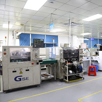
AI hardware PCBA covers the processor, accelerator and carrier boards behind AI servers, edge inference boxes and machine-vision systems. Kilandu builds these higher-density assemblies turnkey in Shenzhen, where BGA-heavy boards are placed on high-speed SMT lines and reflowed with lead-free paste.

- BGA-heavy, high-density processor boards
- X-ray inspection for BGA and hidden joints
- Prototype and volume on the same lines
- Thermal design for compute-heavy boards
- Controlled-impedance stack-up assembly
Capability
What Kilandu can build, test and ship for this product family.
| Parameter | Capability |
|---|---|
| Focus | BGA-heavy, high-density board assembly with X-ray inspection |
| Service | Turnkey PCBA - component sourcing, SMT, DIP, assembly and test |
| Inspection and records | AOI, X-ray for BGA and functional test on customer-specific fixtures, with traceable records issued for every batch |
Applications
Where these higher-density boards are used.
- 01
Edge inference boxes
Compact inference hardware that packs a processor, memory and power delivery into a fan-cooled enclosure.
- 02
AI servers and accelerators
Accelerator and carrier boards where hundreds of BGA balls sit under each package, so X-ray is the only way to verify the joint.
- 03
Machine vision and inspection systems
Camera and vision-processing boards that combine high-speed interfaces with tight impedance control.
- 04
Smart manufacturing controllers
Edge controllers that run machine-learning models next to the production line, where a thermal design that holds up inside a cabinet matters.
- 05
Test and measurement compute boards
Data-acquisition and compute boards for instrumentation, where mixed-signal accuracy and BGA reliability both matter.
How we build it
From solder paste to tested board, inside our own factory in Shenzhen.
SMT assembly
01005 chips up to BGA and QFN placed on our high-speed SMT lines and reflowed with lead-free paste.
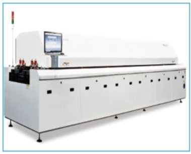
Reflow and wave soldering
Lead-free reflow for SMT, plus our DIP lines with lead-free wave soldering for the through-hole parts.
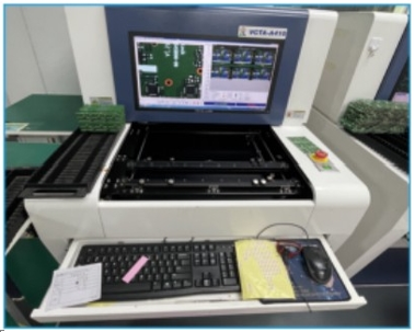
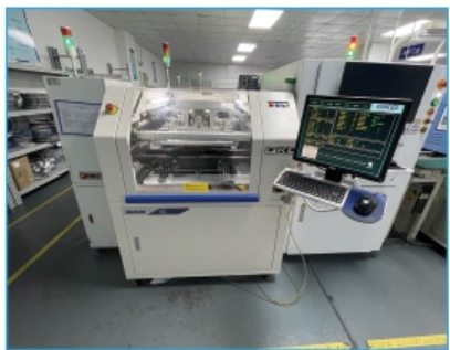
SPI, AOI, X-ray and ICT
3D SPI verifies solder paste volume before placement, AOI inspects every board after reflow, X-ray covers BGA and hidden joints, and in-circuit test runs on fixtures built to your netlist.
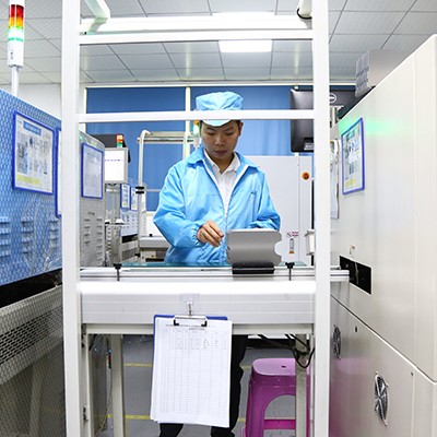
Functional test and traceability
Functional test against your own specification, with traceable inspection records issued for every batch.
Frequently Asked Questions
Quick answers to what buyers ask us most about this product family.
Can you assemble BGA-heavy AI hardware boards?
Yes. AI hardware boards are dense, BGA-heavy assemblies, so they run through our high-speed SMT lines with AOI and X-ray inspection for BGA, then functional test before packing.
Do you support both prototype and volume quantities of compute boards?
Yes. Most AI hardware projects start with prototype or pilot quantities to validate the design and our process, then ramp to volume on the same lines, so the process, materials and test method stay unchanged between the two stages.
Which quality system covers your AI hardware PCBA?
Orders run through a certified quality system with IPC-A-610 Class 2/3 acceptance criteria and RoHS/REACH-compliant processes. Traceable inspection records covering solder paste, reflow profile, AOI and final functional test are issued with every batch.
What is the lead time for a high-density AI board?
For most AI hardware assemblies, 2 to 5 weeks from the point the BOM and Gerber are confirmed and components are released, depending on laminate and BGA material lead times and whether test fixtures have to be built first.
Can you handle high layer counts and fine-pitch BGA?
Yes. Kilandu assembles boards from 1 to 24 layers with fine-pitch placement down to 01005 and 0.25 mm pitch. Hidden joints such as BGA and QFN are verified by X-ray, and controlled-impedance traces are checked against the customer stack-up before production.
How is thermal management handled on high-power AI boards?
Through copper weight and via design agreed at DFM stage: heavy copper inner layers, thermal via arrays under power devices, and where required metal-core or thick-copper constructions. Assembly side, we follow the customer reflow profile for high-mass boards rather than a default profile.
Send us your Gerber and BOM
We will come back with a turnkey quotation - PCB, components, assembly and test - usually within one working day.