
PCBA (Printed Circuit Board Assembly) is the process of soldering electronic components to printed circuit boards to make electronic components with specific functions.

The following are the main steps of PCBA production:
I. Design and preparation
a. Circuit design
According to the functional requirements of the product, use electronic design automation (EDA) software for circuit schematic design and PCB layout design. Ensure the correctness, reliability and manufacturability of the circuit, and consider factors such as component selection, layout, and wiring.
b. Material procurement
According to the design documents, determine the required electronic components list and purchase them. Select reliable suppliers to ensure the quality and delivery cycle of components.
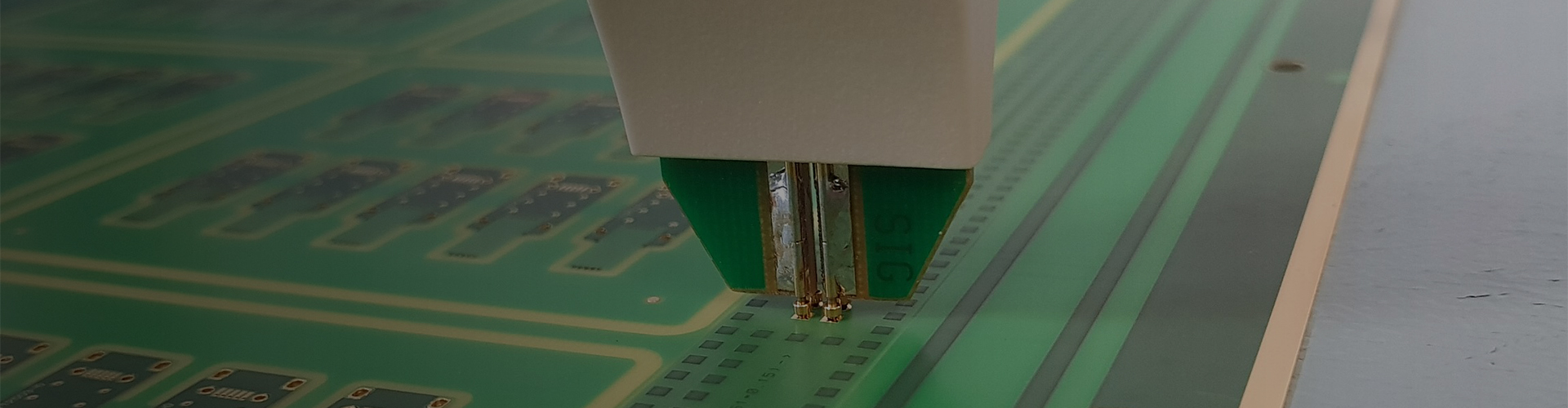
c. PCB production
Send the designed PCB files to the PCB manufacturer for production. The PCB manufacturing process includes processes such as photolithography, etching, drilling, and electroplating to produce printed circuit boards that meet the design requirements.
II. SMT patch
a. Solder paste printing
Print the solder paste onto the pads of the PCB through the steel mesh to prepare for the soldering of components. The quality of solder paste printing directly affects the effect of soldering, and the thickness, uniformity and position accuracy of the solder paste need to be controlled.
b. Component placement
Use a placement machine to accurately place electronic components on the pads on the PCB. The placement machine picks up components through devices such as vacuum nozzles or robotic arms, and places the components on the PCB according to a pre-set program.
c. Reflow soldering
Put the PCB with mounted components into the reflow soldering furnace, heat it to melt the solder paste, and then solder the components to the PCB. The temperature curve of the reflow oven needs to be set according to the characteristics of the solder paste and the requirements of the components to ensure the quality of welding.
Three, plug-in and welding
a. Plug-in
For some electronic components that are not suitable for SMT patches, such as plug-in resistors, capacitors, inductors, etc., manual plug-in is required. When plugging in, pay attention to the direction and position of the components to ensure correct insertion.
b. Wave soldering
The inserted PCB is passed through a wave soldering machine to make the PCB contact with the molten solder to achieve the soldering of the inserted components. The quality of wave soldering is affected by factors such as solder temperature, wave crest height, and soldering time, and needs to be properly adjusted and controlled.
IV. Inspection and Debugging
a. Appearance Inspection
Perform an appearance inspection on the soldered PCBA to check whether the soldering quality, position accuracy, and marking of the components meet the requirements. Appearance inspection can be performed by naked eye observation or using tools such as magnifying glasses and microscopes.
b. Electrical performance test
Use test equipment to test the electrical performance of PCBA, including conductivity test, insulation resistance test, functional test, etc. Electrical performance test can ensure that the circuit connection of PCBA is correct and the function is normal.
c. Debugging and repair
If problems are found during the test, debugging and repair are required. Debugging can be carried out through software debugging, hardware debugging, etc., and repair requires welding, replacement of components, etc. according to the specific problems.
V. Packaging and Delivery
a. Cleaning and three-proofing treatment
Clean the PCBA to remove residual flux, impurities, etc. Perform three-proofing treatment as needed, namely moisture-proof, mildew-proof, and salt spray-proof treatment to improve the reliability and service life of the PCBA.
b. Packaging
PCBA is packaged, usually with anti-static bags, foam boxes, cartons and other packaging materials to protect the PCBA from damage during transportation and storage.
VI. Delivery
Deliver the packaged PCBA to the customer or proceed to the next step of assembly and production. PCBA production is a complex process that requires strict quality control of each link to ensure the quality and reliability of the final product. At the same time, with the continuous development of electronic technology, PCBA production is also constantly innovating and improving, such as using higher-precision placement machines, more advanced welding technology, and automated testing equipment to improve production efficiency and product quality.
PCBA (Printed Circuit Board Assembly) products refer to finished products after assembling electronic components on a bare printed circuit board (PCB, Printed Circuit Board). PCBA is an important link in the manufacturing process of electronic products and a key part in realizing the functions of electronic products.
PCBA manufacturing process
PCB design:
The first step in making a PCBA is to design a printed circuit board (PCB). Engineers use specialized software (such as Altium Designer, Eagle, etc.) to design the layout of the circuit board, including the placement of components, wiring, and electrical connections. After the design is completed, the Gerber file for manufacturing the PCB is generated.
PCB manufacturing:
PCB is manufactured according to the design file. This step involves processes such as printing copper layer, etching, drilling and coating insulation layer. The manufactured PCB board is usually a bare board without any components.
Component procurement:
According to the design requirements of PCBA, purchase the required electronic components, such as resistors, capacitors, diodes, integrated circuits (ICs), etc. The selection of components needs to consider factors such as quality, price, and delivery cycle.
SMT patch (Surface Mount Technology):
SMT patch is the process of installing electronic components on PCB boards through automated equipment. First, solder paste is applied to the surface of the PCB, and then the components are placed in the correct position through the placement machine. Next, the PCB passes through a reflow soldering oven, and the solder paste melts and solidifies at high temperature to fix the components.
DIP plug-in (Through-Hole Technology, THT):
Some components (such as transformers, large capacitors, etc.) cannot use SMT technology. They need to be inserted into the holes of the PCB manually or by machine through the DIP plug-in process, and then fixed by wave soldering or manual soldering.
Inspection and testing:
After the PCBA is manufactured, functional testing and quality testing are required. Common inspection methods include AOI (Automated Optical Inspection), X-ray inspection and functional testing to ensure that the circuit board can work properly and meet the design specifications.
Assembly and packaging:
After completing the test and confirming that the PCBA is correct, the PCBA will be installed in the product's housing for final assembly and packaging to become a complete electronic product.
Application fields of PCBA products
PCBA products are widely used in various electronic products, including but not limited to:
Consumer electronics: such as smart phones, tablet computers, TVs, etc.
Industrial control: such as automation control systems, industrial robots, PLCs, etc.
Medical equipment: such as blood pressure monitors, electrocardiographs, diagnostic equipment, etc.
Automotive electronics: such as automotive electronic control units (ECUs), in-car entertainment systems, sensors, etc.
Communication equipment: such as routers, switches, base station equipment, etc.
Challenges and future of PCBA products
Miniaturization and high-density wiring: With the trend of miniaturization of electronic products, PCBA needs to support more functions and higher integration, which puts higher requirements on design and manufacturing.
Cost control: Under the premise of ensuring product quality, how to reduce production costs is always one of the challenges faced by PCBA manufacturers.
Reliability and quality control: PCBA usually needs to work in various environments, and ensuring its stability and reliability under conditions such as high temperature, humidity, and vibration is a key issue.
Environmental requirements: With the increasingly stringent environmental regulations, the PCBA manufacturing process needs to meet environmental requirements such as lead-free soldering to reduce the impact on the environment.
In the future, with the development of technologies such as 5G, Internet of Things, and artificial intelligence, PCBA will further play a role in a wider range of fields and promote the development of electronic products towards a smarter and more efficient direction.