
Product Category: Multi-Channel Signal Acquisition and Processing PCBA
Number of Layers: Two-layer
Dimensions: Approximately 165mm × 95mm
Surface Finish: Lead-Free Halogen-Free (HASL)
Base Material: FR-4 with Green Solder Mask
Assembly Method: SMT + DIP
I. Product Features
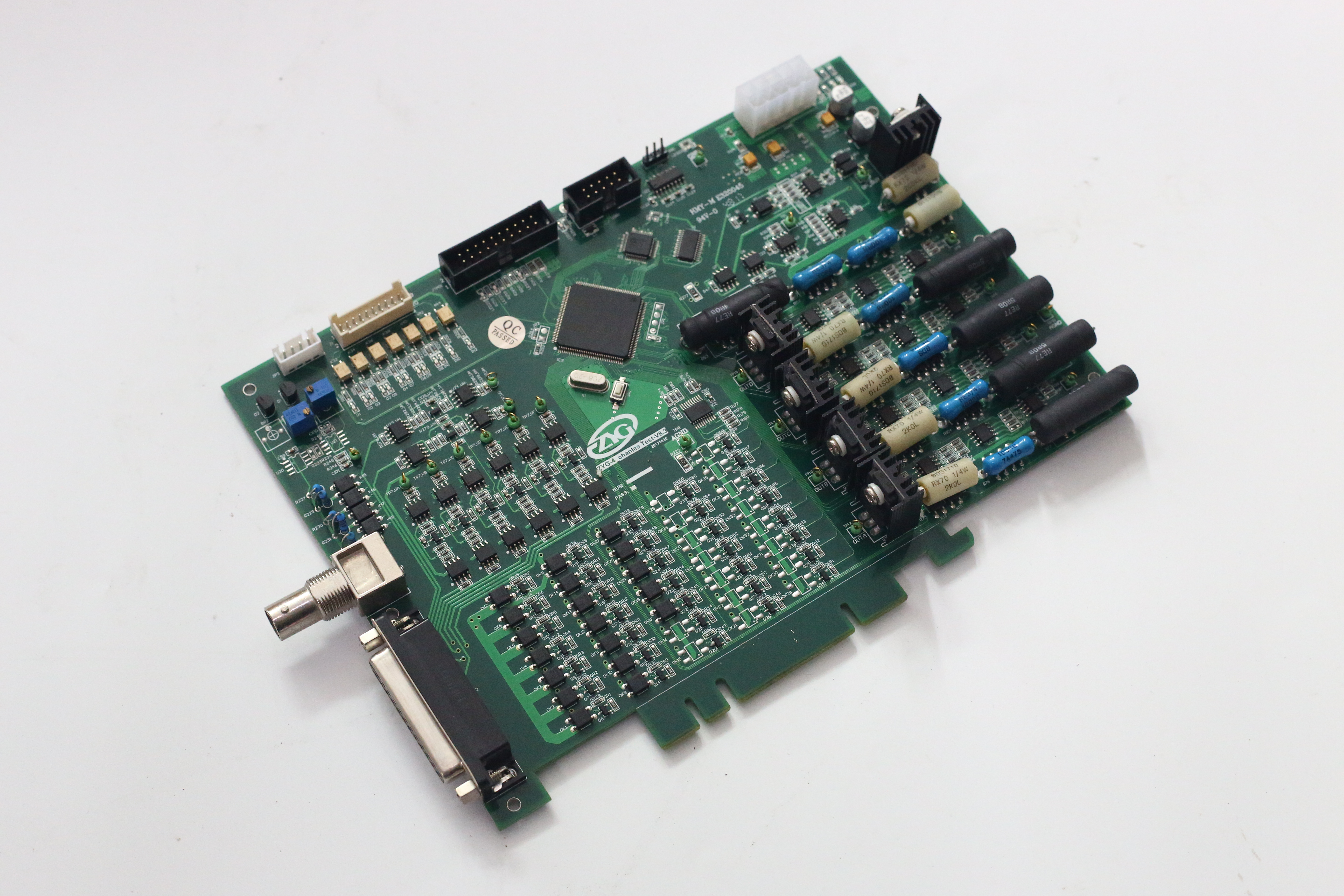
1. Signal Acquisition and Processing Core
The center of the board features a large-scale integrated circuit (QFP) chip, which could be an FPGA, DSP, or high-performance MCU, responsible for multi-channel signal acquisition, processing, and output control.
Surrounding the chip are multiple arrays of chip resistors, capacitors, and op amp/comparator arrays for analog signal conditioning and filtering.
2. Multi-Channel Input Interface
The right side features a row of five 3.5mm audio jacks (with coupling capacitors and protection components) suitable for receiving multiple analog signals (such as sensors, probes, or audio inputs).
Each input channel has its own independent protection resistor, capacitor, and possibly an op amp buffer to ensure signal stability and interference immunity.
3. Data Communication and Expansion
The lower left corner of the board features a BNC coaxial connector (analog/high-speed signal input and output), alongside a DB25 connector for parallel transmission of multiple signals or control signal expansion.
Multiple black pin headers are located on the top of the board for connecting to external expansion boards or the host system.
4. Power Management and Power Supply
A 4-pin white power supply connector is located on the top right side of the board, along with a power filter inductor and electrolytic capacitors. These connectors may support either a 5V or 12V power input.
Multiple voltage regulator chips are included on the board, providing independent regulated power supplies for the core chips and analog front end.
5. High-Density Signal Conditioning Area
The center left corner of the PCB features a dense distribution of surface-mount op amps/comparator chips (SOP packages), which, along with discrete components, form circuits for signal amplification, filtering, and limiting.
This area is directly connected to the multi-channel input ports, indicating its primary function is front-end signal conditioning.
II. Application Scenarios
Multi-channel Data Acquisition (DAQ) Cards
Medical Monitoring Equipment (ECG and EEG Multi-channel Acquisition)
Acoustic or Vibration Signal Analysis Systems
Industrial Sensor Array Signal Processing
Signal Acquisition and Recording for Scientific Research Experiments
Automated Test Systems (ATE)
Product Category: Multi-Channel Signal Acquisition and Processing PCBA
Number of Layers: Two-layer
Dimensions: Approximately 165mm × 95mm
Surface Finish: Lead-Free Halogen-Free (HASL)
Base Material: FR-4 with Green Solder Mask
Assembly Method: SMT + DIP
I. Product Features
1. Signal Acquisition and Processing Core
The center of the board features a large-scale integrated circuit (QFP) chip, which could be an FPGA, DSP, or high-performance MCU, responsible for multi-channel signal acquisition, processing, and output control.
Surrounding the chip are multiple arrays of chip resistors, capacitors, and op amp/comparator arrays for analog signal conditioning and filtering.
2. Multi-Channel Input Interface
The right side features a row of five 3.5mm audio jacks (with coupling capacitors and protection components) suitable for receiving multiple analog signals (such as sensors, probes, or audio inputs).
Each input channel has its own independent protection resistor, capacitor, and possibly an op amp buffer to ensure signal stability and interference immunity.
3. Data Communication and Expansion
The lower left corner of the board features a BNC coaxial connector (analog/high-speed signal input and output), alongside a DB25 connector for parallel transmission of multiple signals or control signal expansion.
Multiple black pin headers are located on the top of the board for connecting to external expansion boards or the host system.
4. Power Management and Power Supply
A 4-pin white power supply connector is located on the top right side of the board, along with a power filter inductor and electrolytic capacitors. These connectors may support either a 5V or 12V power input.
Multiple voltage regulator chips are included on the board, providing independent regulated power supplies for the core chips and analog front end.
5. High-Density Signal Conditioning Area
The center left corner of the PCB features a dense distribution of surface-mount op amps/comparator chips (SOP packages), which, along with discrete components, form circuits for signal amplification, filtering, and limiting.
This area is directly connected to the multi-channel input ports, indicating its primary function is front-end signal conditioning.
II. Application Scenarios
Multi-channel Data Acquisition (DAQ) Cards
Medical Monitoring Equipment (ECG and EEG Multi-channel Acquisition)
Acoustic or Vibration Signal Analysis Systems
Industrial Sensor Array Signal Processing
Signal Acquisition and Recording for Scientific Research Experiments
Automated Test Systems (ATE)