

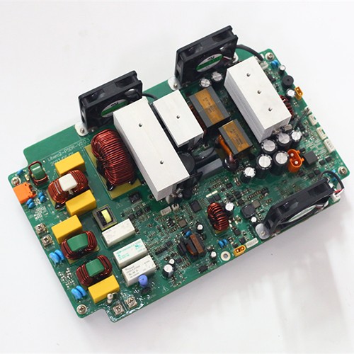
Thick copper PCB
- Product Category: Thick Copper PCB
- Number of Layers: 1-32 (or higher in special stack-up)
- Copper Block: 3 to 20 oz (custom quote is higher)
- Minimum Drill Size: 0.012"
- Maximum Hole Aspect Ratio: 30:1
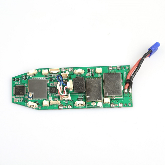
Power system thick copper PCB
- Product Name: Thick Copper PCB
- Thickness: 112um
- Number of Layers: 1+8+1
- Sheet: FR4 Tg170
- Board Thickness: 1.6mm
- Panel Size: 121.6*95mm/2
- Surface Treatment: HASL, OSP, immersion gold, immersion silver
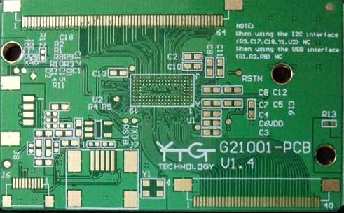
Battery management system (BMS) thick copper PCB
- Product Name: Thick Copper PCB
- Thickness: 108um
- Number of Layers: 1+4+1
- Sheet: FR4 TG150
- Board Thickness: 1.6mm
- Panel Size 105*95mm/1
Heavy Copper and Metal Core Boards for Power Assemblies
On a low-power board copper is a conductor. On a power board it is a conductor, a heatsink and sometimes a structural element, and the board design has to satisfy all three at once. Heavy copper fabrication exists to make that possible, and the decisions that follow from it reach into the assembly process as much as into the fabrication shop.
What heavy copper changes
- Current carrying capacity. A track of a given width carries far more current at 4 oz than at 1 oz, which allows a power stage to be built without busbars or with fewer of them.
- Thermal spreading. Copper under and around a device moves heat into the board, where it can be dissipated over a larger area rather than concentrated at the junction.
- Etching limits. The thicker the copper, the coarser the minimum trace width and spacing, so routing density and copper weight trade against each other and have to be agreed together.
- Assembly thermal load. A board with heavy internal planes takes longer to heat and longer to cool, which changes the reflow profile the assembly needs.
Getting heat out of a power device
The usual route is a combination of copper area under the device, a thermal via array connecting that copper to an internal or opposite-side plane, and an exposed pad or a heatsink on the far side. Each element has to be specified with the others: a via array without adequate copper area on the far side moves heat into a bottleneck, and an exposed pad without a thermal interface material specified at assembly leaves an air gap where the path should be. Because fabrication, assembly and final fitting sit in one factory, that chain is specified as one rather than split between suppliers who each see only their part.
Where heavy copper boards are used
Motor drives and variable frequency equipment, battery management and charging circuits, high-current power supplies, LED drivers and lighting, welding and induction equipment, and industrial power stages generally. In many of these the board also has to meet an acceptance class above the general industrial standard, so the assembly runs to IPC-A-610 Class 2 or Class 3 as agreed at quotation.
Assembling a heavy board
Heavy copper boards usually mix fine-pitch control components with coarse, high-mass power components, and the two are soldered differently. Placement runs the fine-pitch parts first, then through-hole and heavy content is soldered by wave or selective soldering as the board allows. The reflow profile is set for the board thermal mass, and where a heatsink, thermal pad or mounting hardware is part of the finished unit, that is fitted and tested in the same work order. Metal core and ceramic alternatives, which solve a similar thermal problem by a different route, are covered under special board constructions.
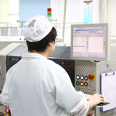
- Factory environment
What heavy copper changes in the process
Heavy copper and metal core boards for current carrying and thermal management, fabricated with copper weights from 2 oz upward and assembled in the same factory. Copper weight, thermal via design and reflow profile are agreed together before the boards are ordered.
Where power and current-carrying boards are used
Each application area has its own assembly requirements. What changes from a medical instrument to a motor drive is the process, the acceptance class and the design rules that matter, and the pages below set out what is different about each one.