

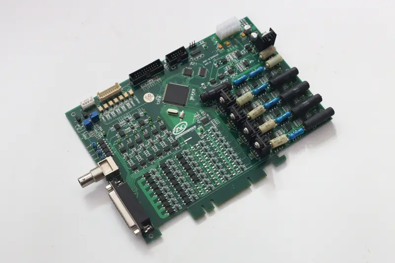
Multi-Channel Signal Acquisition and Processing PCBA
- A multi-channel data-acquisition board for an industrial sensing front-end: typically 4 layers, ~350 components, built as a…
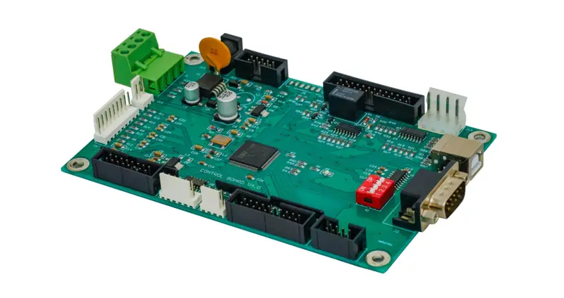
Universal control motherboard (MCU control + peripheral interface)
- A general-purpose control motherboard centred on an MCU with UART/SPI/I2C/CAN peripherals: typically 4–6 layers, ~400 components, pilot…
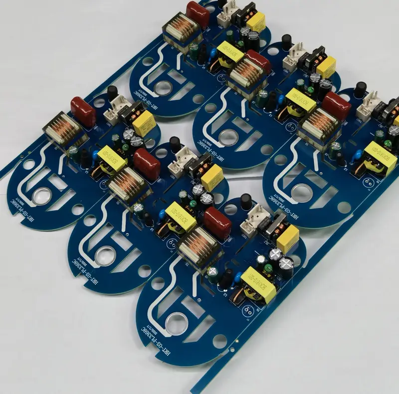
Power drive and voltage conversion circuit board
- A power stage combining MOSFET drive and DC-DC conversion: typically 2–4 layers with heavy copper, ~250 components, pilot run. High current…
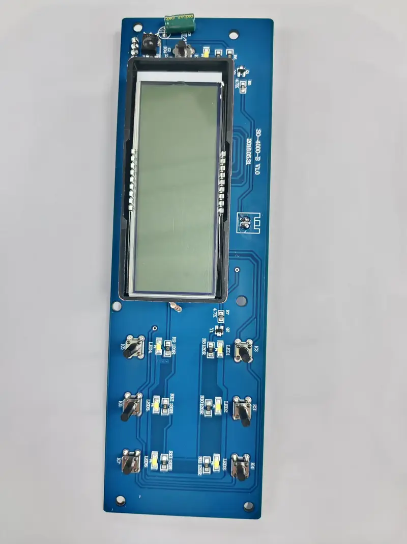
LCD Display Control Panel PCBA
- An HMI control panel driving an LCD with touch and backlight: typically 4 layers, ~300 components, prototype build. Signal integrity for…
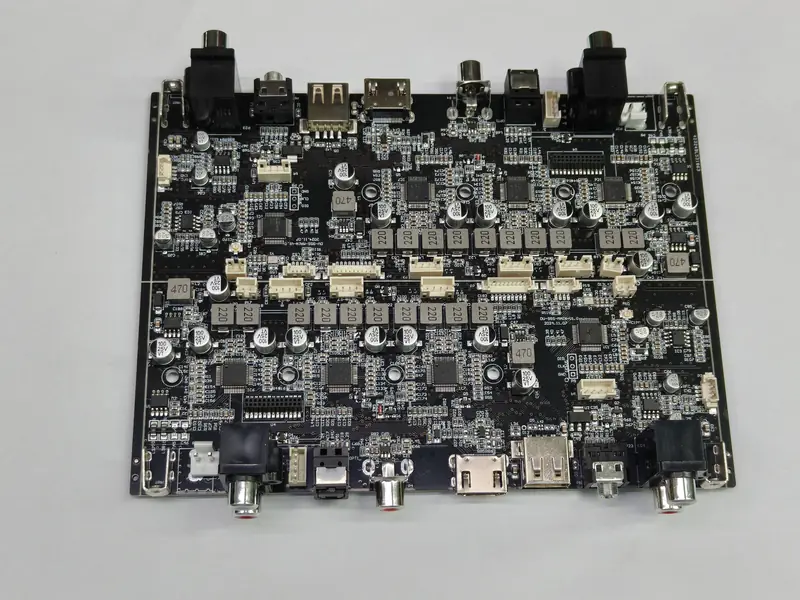
Audio amplifier control motherboard
- A Class-D audio amplifier control board: typically 4 layers, ~280 components, pilot build. Low distortion and stable power delivery define…
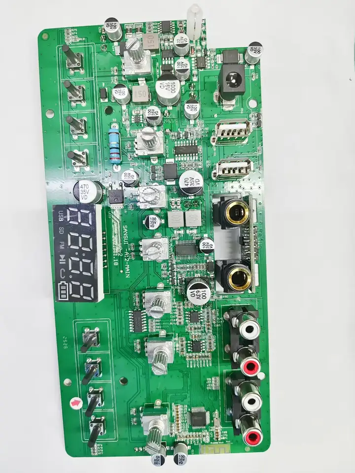
Multifunctional Audio Amplifier PCBA
- A multifunction audio board combining amplifier, mixing and control: typically 4 layers, ~320 components, pilot run. Multiple analog paths…
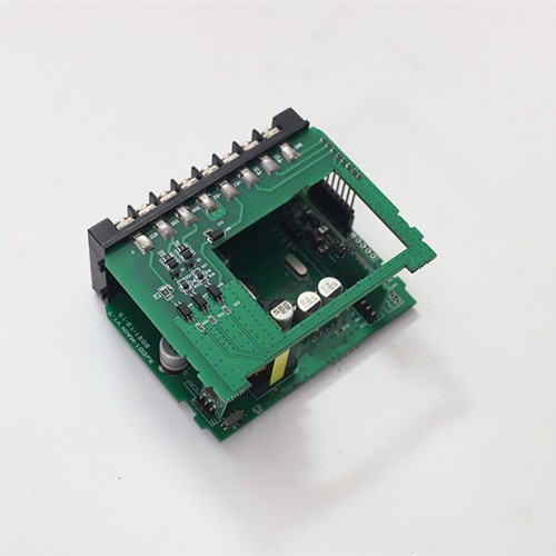
Lithium battery test monitoring system---inverter energy storage PCBA
- It adopts computer-style design, which improves safety and has over-temperature protection, overload protection, low voltage protection, high voltage protection, impact protection, and short circuit protection functions.
High-Density PCBA with BGA and Fine-Pitch Packages
Density changes the nature of assembly. On a board carrying 0402 parts and a handful of SOICs, most defects are visible and most of them can be corrected after the fact. On a board carrying BGA and QFN packages at fine pitch, the joints that matter most are the ones nobody can see, and the cost of discovering a defect at final test is far higher than the cost of preventing it at setup.
What a dense board needs from the assembly process
- Vision-aligned placement for BGA and QFN packages, with component placement from 01005 upward and pitches down to 0.25 mm.
- Dedicated reflow profiles for high-mass and mixed-density boards, verified with thermocouples where the design warrants it rather than inherited from simpler work.
- X-ray inspection of all hidden joints as part of the standard process, with images retained against the lot.
- Controlled handling for moisture sensitive packages, including dry storage and floor-life control before reflow.
- BGA rework capability for the boards where rework is economically right rather than scrap.
Where dense-board defects come from
On a fine-pitch board the defect rate is dominated by three things, and only one of them is the placement machine. The first is paste volume: a stencil aperture that is too small for the pad starves the joint, and one that is too large bridges it, which is why paste volume is measured with 3D SPI rather than checked by eye. The second is thermal: a large package surrounded by small parts needs the surrounding area protected while the package itself reaches reflow, and a board with heavy copper planes needs more heat than its size suggests. The third is moisture, since a package that has absorbed moisture and is reflowed outside its floor-life window will crack internally and fail later rather than at test. All three are controlled by process, and all three are cheaper to control than to detect.
Design decisions that decide the yield
Thermal pads without an adequate via array, via-in-pad that is not filled and capped, solder mask defined pads on fine pitch, and an unbalanced copper distribution that warps the board during reflow are the most common reasons a design assembles poorly. Because fabrication and assembly sit in the same supply chain, these are reviewed before the stencils and the boards are ordered, and the fix is usually a small drawing change rather than a process workaround.
How to start
Send the Gerber files, the bill of materials, the stack-up and the quantity, together with any impedance or acceptance class requirement. For boards with large fine-pitch packages, saying so at quotation stage lets the paste, stencil and profile decisions be made against the real board rather than adjusted after the first build. Reflow profile and paste volume control are covered on the SMT assembly page, and hidden-joint verification is part of the testing scope.
Voiding, head-in-pillow and warpage: the three defects that decide a dense board
On a high-density board the joints that matter most sit under the package, so they are judged from X-ray images rather than from the board surface. Three defect types account for most of the trouble. Voiding is the gas that remains in the joint after reflow, and the acceptance question is what void rate, and what maximum single void, the product tolerates at the thermal pad. Head-in-pillow happens when a warped package and a warped board separate slightly as the paste melts, so the ball contacts the paste but does not coalesce with it — the joint passes continuity at first and opens later in the field. Warpage itself is a design and a heat question: unbalanced copper, a large package on a thin board and a profile that heats one side of the board faster than the other all move the board during the critical seconds of reflow. These three are described in the language of IPC-7095, which is the reference used when acceptance criteria are agreed at quotation.
What has to be right before the first build
Dense boards are usually lost at design review rather than at the machine. A thermal pad without a via array, a via-in-pad that is not filled and capped, a stencil aperture that cannot release enough paste for a 0.3 mm ball pitch, an unbalanced copper distribution that will bow the panel — these are raised at file review, before tooling and stencils are ordered. Placement itself is handled by vision-aligned machines that place parts from 01005 upward and packages at pitches down to 0.25 mm, so the practical ceiling on a dense board is set by the design and by paste printing rather than by placement accuracy alone.
Underfill, reballing and rework on a loaded board
Where a package is under mechanical or thermal stress, an underfill or encapsulation step is added after reflow to spread the load from the solder joints into the board. Rework is possible: a BGA or CSP can be removed with a dedicated rework station using a controlled profile, the pads cleaned and re-dressed, and a replacement reflowed under the same profile control. Balls can also be re-dressed on a package — reballing — where the package itself is being reused. On a board that is already populated the constraint is the neighbouring parts: the area around the site is shielded and the profile is narrowed to the smallest window that will still reflow the joints.
Inspection, and what the lot record contains
Paste volume is measured with 3D SPI, placement and visible joints are checked with AOI, and the joints under BGA, CSP, uBGA and QFN packages are checked with X-ray as part of the standard route rather than on request; the images are kept with the lot record. Where a design warrants it, a sample board from the build is cross-sectioned to verify the process itself rather than the individual board. Prototype builds of a dense board typically take 5-8 working days and production 2 to 5 weeks; send the Gerber, BOM and pick-and-place files through the contact page to start.
- Factory environment

What a 0.3 mm pitch board needs from the process
High-density assembly covers the boards where the joints that matter most are the ones nobody can see: BGA, QFN and fine-pitch packages whose solder sits underneath the component. This page sets out what a dense board demands from placement and reflow, how hidden joints are verified, and which design decisions decide the yield.
Application
Each application area has its own assembly requirements. What changes from a medical instrument to a motor drive is the process, the acceptance class and the design rules that matter, and the pages below set out what is different about each one.