

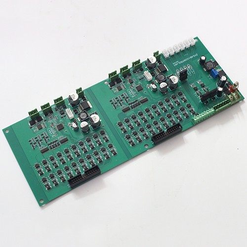
Multilayer PCB
- Product Category: Multilayer PCB
- Material: KB6061, S1141, S1000, IT180, etc.
- Number of layers: 4-48 layers/multilayer PCB
- Solder Mask Color: Green
- Silk Screen Color: White/Black
- Finished Product Thickness: 0.3mm - 6.0mm
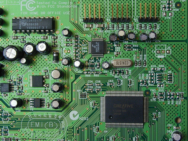
Navigation system motherboard PCB
- Product Name: Multilayer PCB
- Number of layers: 10L
- Sheet: FR4 Tg170
- Board thickness: 2.4mm
- Panel size: 120*95mm/1
- Outer copper thickness: 35μm
- Inner copper thickness: 35μm
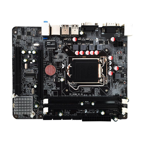
Chassis motherboard PCB
- Product Name: Multilayer PCB
- Number of layers: 12 layers
- Color: Green/White
- Finished product thickness: 1.0mm
- Copper thickness: 2-3OZ
- Surface treatment: immersion gold
Multilayer PCB Fabrication from 4 to 24 Layers
A multilayer board exists because a design has run out of room, and the point at which that happens is usually where the electrical requirements become harder rather than easier. Ground and power planes have to be separated from signals, impedance has to be controlled, and the routing has to reach places the outer layers cannot serve. The board stops being a mechanical carrier and becomes part of the circuit.
What changes as the layer count rises
- 4 to 6 layers covers most industrial, medical and instrumentation boards: a ground plane, a power plane and two to four signal layers, with through vias and standard FR4.
- 8 to 12 layers appears where digital speed, channel count or BGA fan-out demands more routing space, often with controlled impedance on the high-speed nets.
- 14 to 24 layers is where sequential lamination, blind and buried vias and back-drilling enter, and where the stack-up is designed rather than assembled from standard cores.
Stack-up and controlled impedance
On a fast design, the laminate thickness between a signal layer and its reference plane decides the trace impedance, and therefore decides whether the board will work. The stack-up is therefore chosen deliberately: dielectric thickness and material are fixed to hit the target single-ended and differential impedance, and trace widths follow from that rather than being set first. Where a design has a mix of high-speed and low-speed nets, the stack-up is usually arranged so that the high-speed layers sit next to a continuous reference plane, which also helps with return path continuity and emissions.
Vias, lamination and the structures that need them
Blind and buried vias remove via stubs and free routing space on layers that would otherwise be blocked, and microvias allow connections to be made in the outer layers without drilling through the whole board. All of them mean the board is built in more than one lamination cycle, which is a process capability rather than a drawing note. Via fill and via-in-pad are available for designs that need to place components directly over a via, and back-drilling is available where stub length limits the signal integrity budget.
Review before fabrication, not after
Layer count, copper weight, panel design and via structure all feed into assembly: an uneven copper distribution warps during reflow, a tight panel rail damages parts at depanelling, and vias that are not tented or filled can wick solder away from a joint. Because fabrication and the assembly lines sit in the same supply chain, these are checked against the assembly process before the boards are ordered. Send the Gerber files, the stack-up if one exists, the impedance target and the quantity; if no stack-up exists, one is proposed from the design as part of the review.
- Factory environment

Why choose us?
Multilayer bare boards from 4 to 24 layers, fabricated in Baoan District, Shenzhen, with controlled impedance, sequential lamination and heavy copper options. Fabrication and assembly are planned as one chain so the stack-up is reviewed against the assembly process before the boards are ordered.
Application
Each application area has its own assembly requirements. What changes from a medical instrument to a motor drive is the process, the acceptance class and the design rules that matter, and the pages below set out what is different about each one.