

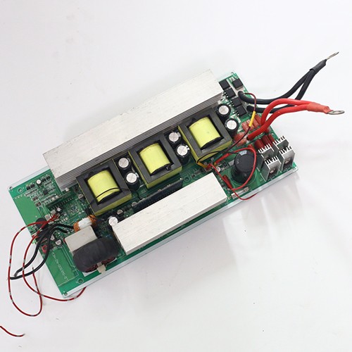
Special board PCB
- Special board PCB is mainly used in special application scenarios such as high frequency and high reliability.
- Special board types:
- 1. High frequency materials: such as Panasonic's Megtron 6, Rogers3003/RT5880, etc., suitable for high frequency signal transmission.
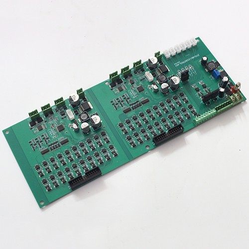
Multilayer PCB
- Product Category: Multilayer PCB
- Material: KB6061, S1141, S1000, IT180, etc.
- Number of layers: 4-48 layers/multilayer PCB
- Solder Mask Color: Green
- Silk Screen Color: White/Black
- Finished Product Thickness: 0.3mm - 6.0mm
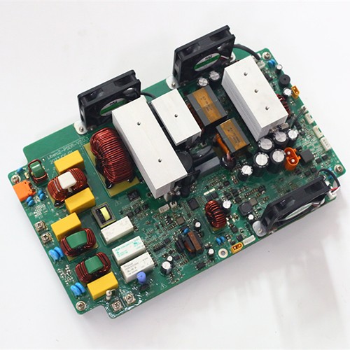
Thick copper PCB
- Product Category: Thick Copper PCB
- Number of Layers: 1-32 (or higher in special stack-up)
- Copper Block: 3 to 20 oz (custom quote is higher)
- Minimum Drill Size: 0.012"
- Maximum Hole Aspect Ratio: 30:1
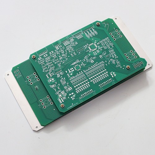
RF PCB
- Product Category: RF / High-Frequency PCB
- Base material: FR-4 / Rogers 4350B / Rogers 4003C / Taconic / hybrid stackup
- Layer count: 2-24 layers (sample: 4 layers)
- Plate thickness: 1.6 +/- 0.25 mm
- Board size: 225.00 mm x 112.00 mm (customizable)
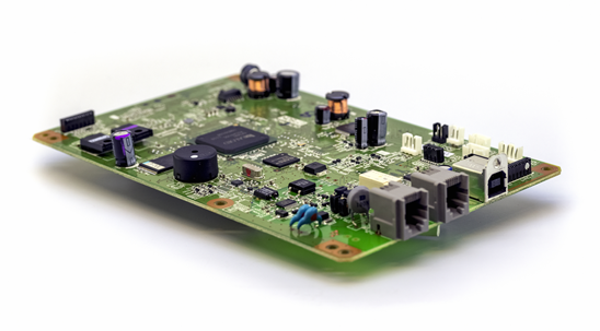
Electronic router RF PCB
- Product Category: RF PCB
- Number of layers: 4
- Size: 225.00mm*108.00mm
- Surface treatment: FR-4
- Board thickness: 0.2mm - 7mm
- Aperture: 0.02mm
- Line width: 0.003
- Line spacing: 0.003
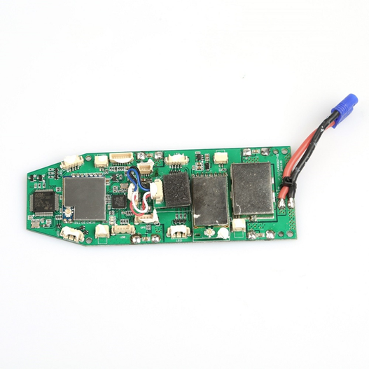
Power system thick copper PCB
- Product Name: Thick Copper PCB
- Thickness: 112um
- Number of Layers: 1+8+1
- Sheet: FR4 Tg170
- Board Thickness: 1.6mm
- Panel Size: 121.6*95mm/2
- Surface Treatment: HASL, OSP, immersion gold, immersion silver
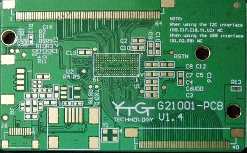
Battery management system (BMS) thick copper PCB
- Product Name: Thick Copper PCB
- Thickness: 108um
- Number of Layers: 1+4+1
- Sheet: FR4 TG150
- Board Thickness: 1.6mm
- Panel Size 105*95mm/1
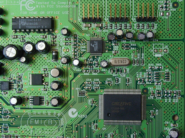
Navigation system motherboard PCB
- Product Name: Multilayer PCB
- Number of layers: 10L
- Sheet: FR4 Tg170
- Board thickness: 2.4mm
- Panel size: 120*95mm/1
- Outer copper thickness: 35μm
- Inner copper thickness: 35μm
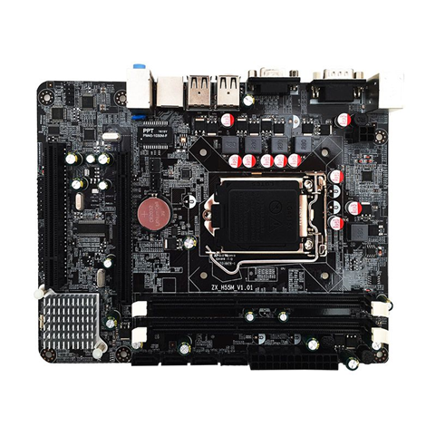
Chassis motherboard PCB
- Product Name: Multilayer PCB
- Number of layers: 12 layers
- Color: Green/White
- Finished product thickness: 1.0mm
- Copper thickness: 2-3OZ
- Surface treatment: immersion gold
Bare Board Fabrication from 1 to 24 Layers
The bare board is the part of a PCBA programme that is easiest to treat as a commodity and hardest to replace once it is wrong. Layer count, laminate, copper weight, surface finish and panel design are all fixed before the first board is etched, and each of them constrains what the assembly process can do later.
What the fabrication range covers
- Layer count from 1 to 24 layers, single-sided through to multilayer with controlled impedance.
- Laminate options including standard FR4, high Tg FR4 for boards that see repeated thermal cycling or lead-free reflow, heavy copper for current carrying and thermal spreading, and aluminium or metal core for insulated metal substrate constructions.
- Surface finishes: lead-free hot air solder levelling, electroless nickel immersion gold, immersion silver and organic solderability preservative.
- Solder mask and legend to the customer specification, with panel design reviewed for assembly yield before release.
Choosing a finish that survives the assembly process
The surface finish is a decision about what happens in the weeks after fabrication, not only about what happens in the plating tank. ENIG gives a flat surface well suited to fine-pitch and BGA placement and a long shelf life, but it costs more and needs the nickel and gold thickness controlled. Lead-free HASL is economical and robust for boards with generous pitch and through-hole content. Immersion silver suits fine pitch where the storage window is short. OSP is the cheapest option and the most sensitive to handling and time. Selecting the finish from the assembly route and the storage window avoids the common situation where a board is perfectly fabricated and still solders badly.
Fabrication and assembly as one chain
Copper weight, panel design and layer stack-up all feed into assembly: a panel that is awkward to depanel damages parts, a heavy copper plane changes the reflow profile, and a stack-up that ignores controlled impedance turns into a test failure rather than a fabrication failure. Because fabrication and the SMT lines sit in the same supply chain, these are reviewed against the assembly process before the boards are ordered. If a design would benefit from a different panel or a different finish, that is raised at review stage, when changing it is still cheap.
Documentation and traceability
Boards carry lot traceability, and material declarations for RoHS and REACH are available with the shipment. For buyers running automotive or medical programmes, inspection records and material documentation can be issued in the form the audit expects. Fabrication usually runs as the first stage of a turnkey PCBA order, where the board and the assembly share one material plan and one set of milestones.
PCB categories
By construction
- Multi-layer PCB — 4 to 24 layers with controlled impedance and sequential lamination.
- Thick copper PCB — heavier copper weights for current carrying and thermal spreading.
By material and performance
- RF PCB — low-loss laminates and hybrid stack-ups for high-frequency designs.
- High-Tg PCB — laminates for repeated thermal cycling and lead-free assembly.
- Special board PCB — metal core, ceramic, flexible and rigid-flex constructions.
- Factory environment

Why choose us?
Bare board fabrication from 1 to 24 layers in Baoan District, Shenzhen, in FR4, high Tg laminate, heavy copper, aluminium and metal core, with the surface finish chosen for the assembly process that follows. Fabrication and assembly are planned as one chain.
Application
Each application area has its own assembly requirements. What changes from a medical instrument to a motor drive is the process, the acceptance class and the design rules that matter, and the pages below set out what is different about each one.