
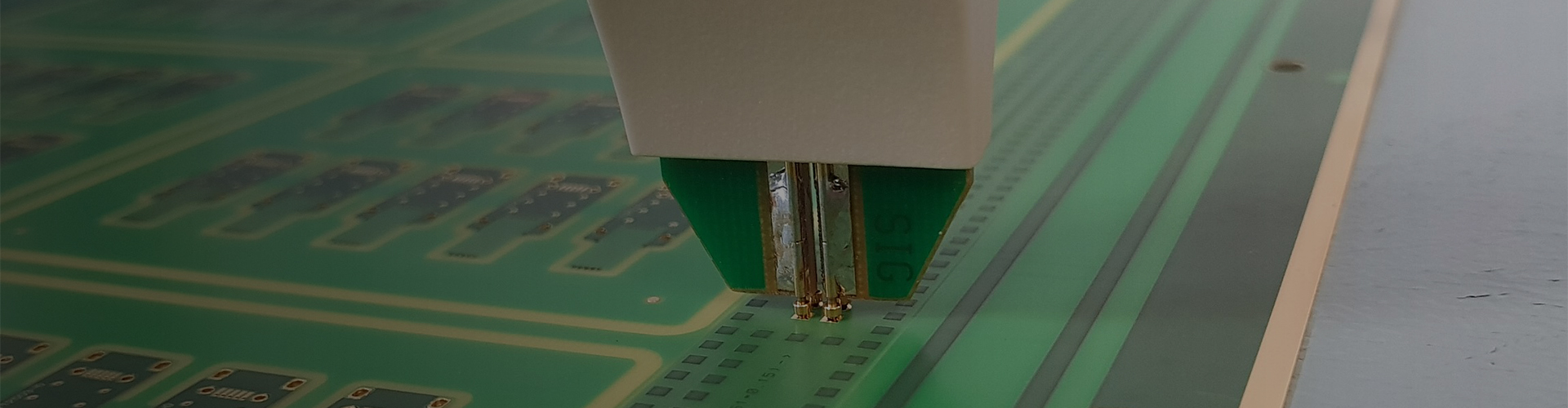
Kilandu's PCBA product range spans SMT, through-hole (DIP), box build and full turnkey assembly for industrial, automotive, medical and IoT devices - from prototype to volume, with managed component sourcing and a certified quality system.
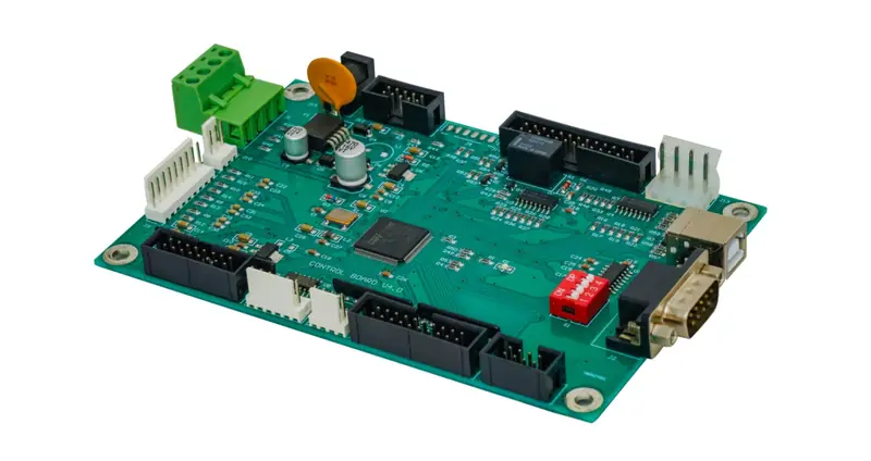
- SMT, DIP, box build and turnkey assembly
- 01005 up to BGA and QFN placement
- Managed sourcing from LCSC and global distributors
- Prototype to 100k+ pcs per month
- SPI / AOI / X-ray / ICT / FCT
Capability
What Kilandu can build, test and ship for this product family.
| Parameter | Capability |
|---|---|
| SMT | 01005-BGA placement |
| THT / DIP | axial / radial |
| Box build | cables, enclosures |
| Volume | prototype to 100k+ pcs/month |
| Test | In-process SPI + AOI + X-ray; electrical ICT + FCT |
| Lead time | 2-5 weeks |
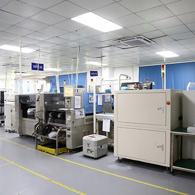
What we build
The assembly services you can buy from one factory.
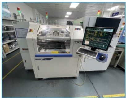
- 01
SMT assembly
01005 chips up to BGA and QFN on our high-speed SMT lines, with AOI on every board.
- 02
Through-hole (DIP) assembly
our DIP lines with lead-free wave soldering for axial and radial parts, plus hand soldering for odd-form components.
- 03
Box build and cable assembly
Cables, enclosures and mechanical assembly, so the shipment arrives ready for your line rather than for your bench.
- 04
Turnkey (full BOM) projects
Component sourcing from LCSC and global distributors with BOM matching and shortage alerts, so you receive a board rather than a kit.
- 05
Prototype and NPI
Small quantities to validate the design and the process, with engineering support before you commit to volume.
How we build it
From solder paste to tested board, inside our own factory in Shenzhen.
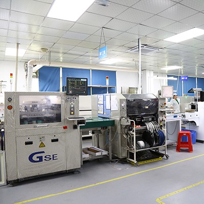
SMT assembly
01005 chips up to BGA and QFN placed on our high-speed SMT lines and reflowed with lead-free paste.
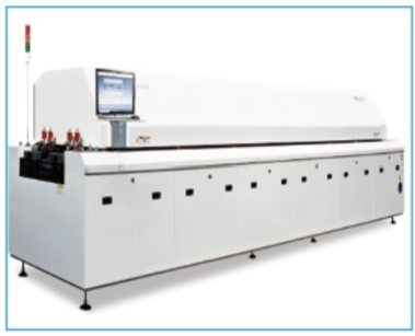
Reflow and wave soldering
Lead-free reflow for SMT, plus our DIP lines with lead-free wave soldering for the through-hole parts.
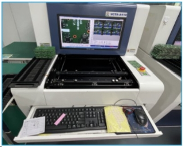
SPI, AOI, X-ray and ICT
3D SPI verifies solder paste volume before placement, AOI inspects every board after reflow, X-ray covers BGA and hidden joints, and in-circuit test runs on fixtures built to your netlist.

Functional test and traceability
Functional test against your own specification, with traceable inspection records issued for every batch.
Frequently Asked Questions
Quick answers to what buyers ask us most about this product family.
What PCBA services does Kilandu offer?
SMT, through-hole (DIP), box build, and full turnkey assembly from prototype to volume.
Do you source components?
Yes - managed sourcing from LCSC and global distributors, with BOM matching and shortage alerts.
What quality standard do you assemble to?
IPC-A-610 Class 2/3 with SPI/AOI/X-ray/ICT/FCT.
What component types and package sizes can you place?
Fine-pitch devices down to 01005 and 0.25 mm pitch, including QFN, BGA, connectors and odd-form parts. Boards from 1 to 24 layers are supported, and mixed-technology assemblies that combine fine-pitch SMT with heavy through-hole parts are handled on the same lines.
What inspection is built into the process?
Solder paste volume is verified by 3D SPI before placement, automated optical inspection runs after reflow, and X-ray is used where joints are hidden, such as BGA and QFN. Final functional test is applied where the customer specifies it, and lot-level traceability links the finished assembly to the material and process records.
Can you build a complete product rather than just the board?
Yes. Box build and final assembly are available, covering enclosure assembly, cable and harness fitting, connector and label application, and the functional test that confirms the finished unit. That lets a customer take delivery of a tested product rather than a board that still needs integration work.
Send us your Gerber and BOM
We will come back with a turnkey quotation - PCB, components, assembly and test - usually within one working day.