

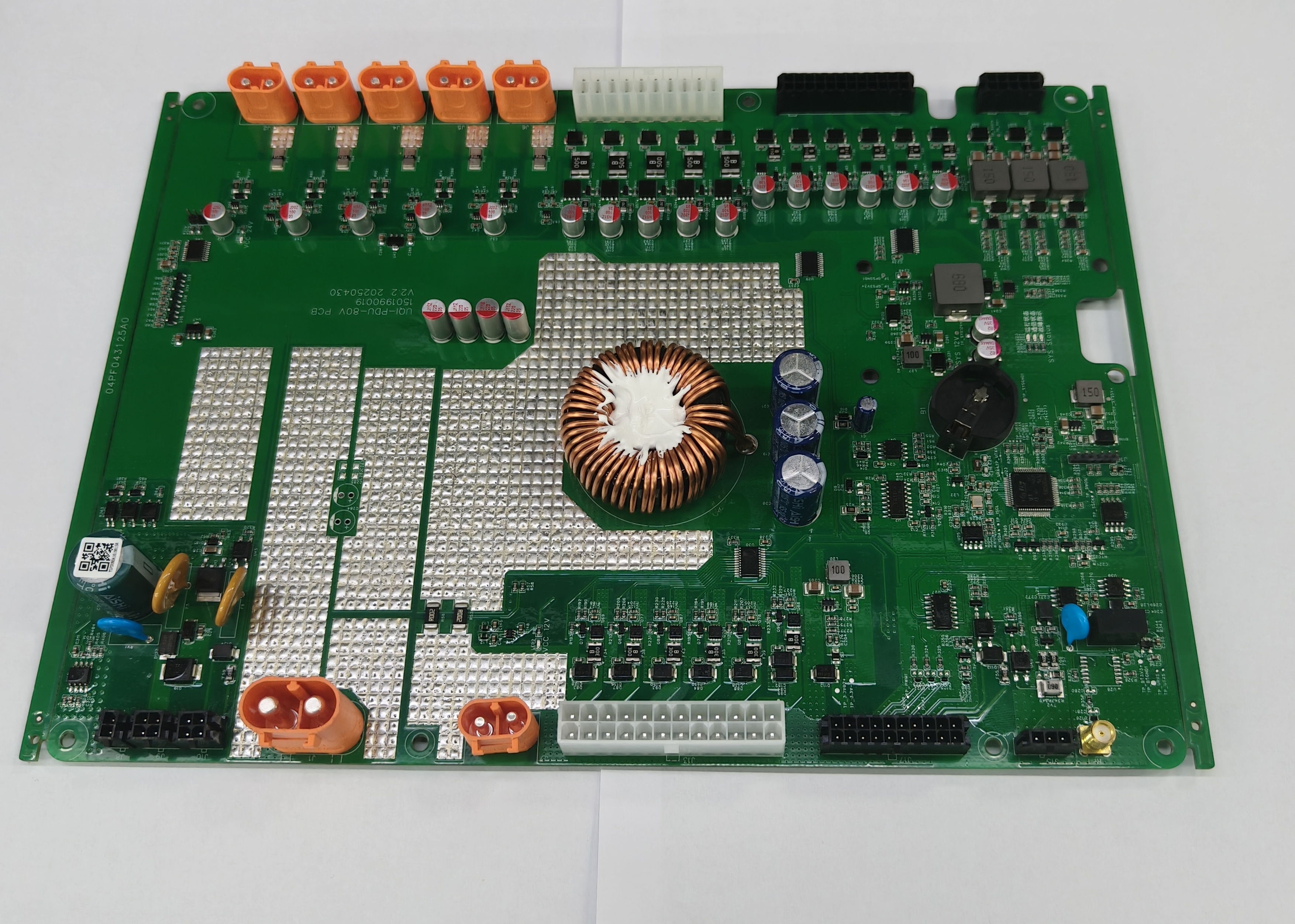
Number of layers: double-layer board
Size: about 290mm × 180mm
Surface treatment: hot air leveling (HASL), pads are silver-white
Base material: FR-4
Assembly type: SMT + DIP mixed
Functional modules and feature analysis:
1. High-voltage and high-current power module
The top row of large orange terminal interfaces indicates that it supports high-voltage and high-current input/output, and is often used for power supply or motor control.
The large inductor + electrolytic capacitor + MOS tube array in the middle of the area is combined with a large area of heat dissipation copper foil. It is judged that this is a DC-DC buck or inverter control module with a certain power handling capacity.
2. Power management module
The multiple inductors, capacitors and power chips on the lower right side form the switching power supply stabilization area, which is responsible for powering the main control and drive parts.
Contains fuses, TVS tubes, etc. for overvoltage and overcurrent protection.
3. Control and logic module
The densely distributed SMD components on the right include:
MCU/main control chip (large package chip below)
RTC (with battery holder)
EEPROM (if any)
Multi-channel MOSFET drive (may be relay/load switching control)
There are debugging interfaces (such as JTAG, SWD, UART), and DIP switch settings.
4. Interface module
Multiple groups of white pins (such as pin headers, terminal blocks), supporting external connections:
Control signal input
Load output
Communication interface (CAN, RS485, SPI, etc.)
The QR code label and SN code in the lower left corner indicate that production traceability and code scanning configuration are supported.
5. Electromagnetic compatibility and heat dissipation
Large area of exposed copper + tinning treatment to improve heat dissipation performance and provide electromagnetic shielding
The yellow X capacitor and lightning protection device in the lower left corner are suspected to exist to enhance anti-interference ability
Applicable scenario suggestions
Based on its design structure and device type, it is speculated that this board can be used for:
Motor drive controller in high voltage/high current scenarios
Energy storage inverter/photovoltaic inverter control unit
New energy vehicle battery management system (BMS) or OBC controller
Industrial-grade power control system