

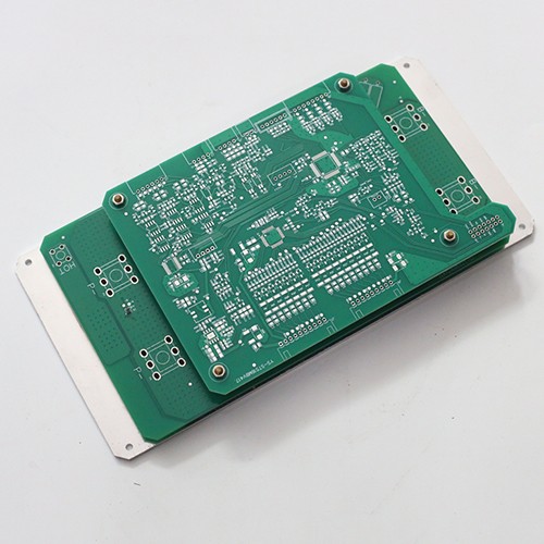
RF PCB
- Product Category: RF / High-Frequency PCB
- Base material: FR-4 / Rogers 4350B / Rogers 4003C / Taconic / hybrid stackup
- Layer count: 2-24 layers (sample: 4 layers)
- Plate thickness: 1.6 +/- 0.25 mm
- Board size: 225.00 mm x 112.00 mm (customizable)
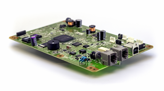
Electronic router RF PCB
- Product Category: RF PCB
- Number of layers: 4
- Size: 225.00mm*108.00mm
- Surface treatment: FR-4
- Board thickness: 0.2mm - 7mm
- Aperture: 0.02mm
- Line width: 0.003
- Line spacing: 0.003
RF and High-Frequency PCB Fabrication
At low frequency a board is a mechanical support for copper that carries signals. As the frequency rises, the board becomes part of the circuit: the dielectric properties of the laminate affect loss and phase, the geometry of a trace sets its impedance, and the reference plane under a signal decides whether the return path is continuous. Fabricating an RF board is therefore a matter of building the electrical design accurately, not just the drawing.
What the RF range covers
- PTFE and low-loss laminate options for the sections where the loss budget or phase stability requires them.
- Standard and high Tg FR4 for digital, control and power sections, laminated with the RF material into a single hybrid stack-up.
- Controlled impedance on single-ended and differential traces, calculated from the built stack-up rather than a generic table.
- Via structures, ground stitching and shielding provisions designed across the boundary between materials.
Material choice and what it costs
Low-loss material is more expensive and slower to process than FR4, so it is used where it changes the result. The usual test is the insertion loss budget together with the phase stability requirement: if the design meets its budget on FR4 at the operating frequency, there is no reason to pay for PTFE. Where the loss or the phase variation across temperature does not fit the budget, the material is not a refinement but a requirement. Because the decision is made at the stack-up stage, the cost is known before the tooling is ordered rather than discovered after a prototype fails.
Hybrid stack-ups and the transition region
A hybrid board is more than two boards laminated together, because the boundary is where most of the risk sits. A reference plane that changes material mid-board changes impedance, ground stitching that stops at the boundary gives the return current no path, and a via that works in one material may need a different treatment in the other. With fabrication and assembly in the same chain, the transition region is designed once, with the assembly process in view, rather than being split between a board shop optimising for its process and an assembler optimising for its own.
Assembly of RF boards
RF assemblies mix fine-pitch components with shielded parts, connectors with specific launch geometry, and often a metal shield can that has to be fitted after reflow. Placement runs the fine-pitch parts first, shield and connector attach are handled in the same work order, and the acceptance class follows the product rather than the frequency. Where a low-loss material or a multi-stage lamination is involved, the fabrication milestone is quoted against the actual stack-up rather than a standard lead time. The assembly side of an RF product, including shielding, coating and RF test, is covered under RF PCBA assembly.
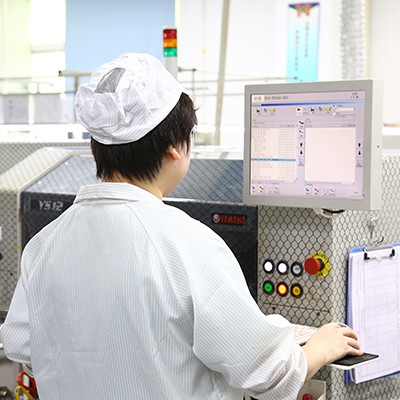
- Factory environment
Why choose us?
RF and high-frequency bare boards fabricated with PTFE and low-loss laminates, controlled impedance and mixed dielectric stack-ups. Frequencies, impedance targets and material choices are agreed from the stack-up before the boards are built rather than after they are measured.
Application
Each application area has its own assembly requirements. What changes from a medical instrument to a motor drive is the process, the acceptance class and the design rules that matter, and the pages below set out what is different about each one.