

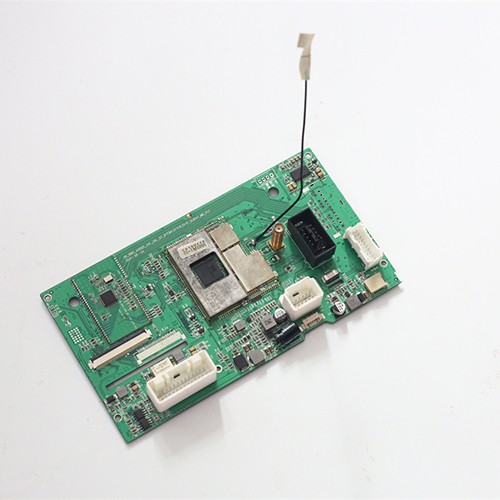
RF Radio Frequency PCBA
- RF PCBA is an electronic assembly that combines RF technology with printed circuit boards (PCBs) and assembles RF components on PCBs through processes such as surface mount technology (SMT).
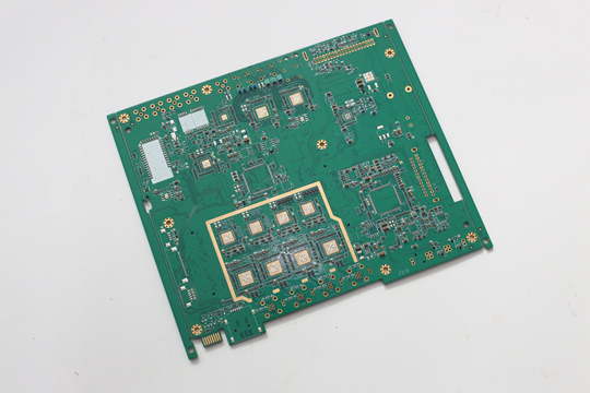
Automobile smart cabin motherboard PCBA
- Automotive intelligent cockpit motherboard PCBA is a key component in modern cars, which is responsible for processing and controlling various electronic devices and functions in the cockpit.
RF and Wireless PCBA Assembly
Assembling an RF board is less about placing parts accurately, which the machine does, and more about not undoing the design. Radio performance is decided by the geometry and the grounding of the RF section, and there are several ordinary assembly decisions that quietly change both: where a shield is fitted, what gets coated, and how much heat the module sees.
What gets specified before the first build
- Which components sit inside a shield and which must stay outside it, and at what point in the sequence the shield is fitted.
- Ground stitching and via placement around the RF section, checked against the module reference layout where one exists.
- Coating coverage and masking, since coating over an antenna area or a tuning element changes the electrical result.
- Thermal profile for a board that mixes fine pitch, a module with its own limits, and often a metal chassis connection.
- Inspection and test plan, including what is checked before a shield is fitted and what is checked at unit level afterwards.
Shields, sequence and heat
The shield can is a small part with a large effect. Fitted before reflow, it adds mass and changes the temperature profile under and around it, and it also means the joints beneath it can never be inspected afterwards. Fitted after reflow, the joints can be X-rayed and recorded but the part is placed by hand or with a press. Neither route is wrong; what matters is deciding before production, when the paste volume, the profile and the inspection plan can be written to match the choice. The same applies to coating: an RF section that is coated by default may lose performance, and one that is masked by default may not meet the environmental requirement of the product.
Mixed technology on an RF board
Most RF assemblies are not RF only. They carry a control section, a power section and often a through-hole connector with a specific launch geometry. Selective soldering applies heat to the through-hole joints only, which keeps the fine-pitch and RF sides away from a second full thermal cycle. The acceptance class then follows the product rather than the frequency: an RF board in an industrial instrument runs to the same IPC-A-610 class as any other industrial assembly.
Proving the assembly works
Continuity is not a useful test on a radio. What matters is whether the link behaves as designed, so the test is agreed from the product function: a transmit and receive check, a current draw measurement, a sensitivity check at a defined input level, or a link test in the final antenna arrangement. Where a customer fixture and specification exist they are used directly, and where they do not, a workable procedure is developed alongside the first build. The bare board this assembly is built on is covered under RF PCB fabrication, and where a design mixes radio and control circuitry on a dense board, see high-density PCBA.
Controlled impedance: what has to survive the assembly process
On an RF board the geometry of a trace is part of the circuit, so the assembly process has to leave it alone. The impedance of a line is set by its width, by the dielectric thickness above and below it and by the copper thickness; a controlled-impedance requirement is normally stated with a tolerance, and holding it through assembly means controlling the press and the drilling of the stack-up, the plating, and the temperatures the laminate sees. On low-loss designs the laminate choice matters as much as the geometry: Rogers and PTFE-based materials behave differently from FR-4 during drilling and reflow and need their own tooling and process window. A 50 ohm line that leaves the fabricator correct can still shift if the board is reflowed twice, or if a shield frame is soldered with more heat than the laminate wants.
Shields, staking and the order of operations
Where a board carries a shield can, the sequence is planned so that nothing is soldered over a joint that still has to be inspected. Joints under the frame are inspected and recorded before the can is fitted, because they are not accessible afterwards. Ground stitching around an RF section is treated as part of the circuit rather than as mechanical detail, and the staking and conformal coating steps are checked against the areas that must stay clear — a coating applied across a matched line changes it.
Mixed technology without disturbing the RF section
RF assemblies usually combine fine-pitch surface mount with through-hole connectors, a shield frame or a chassis connection. Selective soldering is used so the through-hole joints get the heat they need without sending the fine-pitch side and the RF section through a second full thermal cycle, which is also what protects the laminate. Where a module is used rather than a chipset-down design, the module's own keep-out, handling and moisture-sensitivity requirements are written into the process instructions.
Testing: what is measured here, and what belongs to a calibrated bench
Every board goes through AOI, and X-ray covers joints hidden under modules, QFNs and shielded packages; electrical test covers in-circuit test and a functional test at board level. RF performance itself — return loss, insertion loss and VSWR measured with a vector network analyser — is normally verified against the customer's specification, or on a calibrated bench at the customer's end or in a test house, because that measurement depends on the fixture and the instrument rather than on the assembly. What is guaranteed here is that the process has not disturbed the impedance, the ground reference or the shield cavities. Where no RF test specification exists, the practical checks are agreed at quotation: transmit and receive function, current draw, sensitivity at a defined input, or a link test with the final antenna. Prototype builds typically take 5-8 working days and production 2 to 5 weeks.
- Factory environment

What an RF assembly has to protect
RF assembly is less about placing parts accurately, which the machine does, and more about not undoing the design. This page covers how shielded sections, matched lines and module-based radios are carried through placement, soldering, coating and test without the RF section losing performance on the way.
Application
Each application area has its own assembly requirements. What changes from a medical instrument to a motor drive is the process, the acceptance class and the design rules that matter, and the pages below set out what is different about each one.