

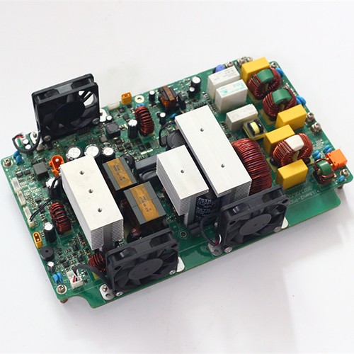
Inverter product motherboard
- The inverter product PCBA is the core component of the inverter, which is responsible for the inverter's signal processing, control logic and drive output.
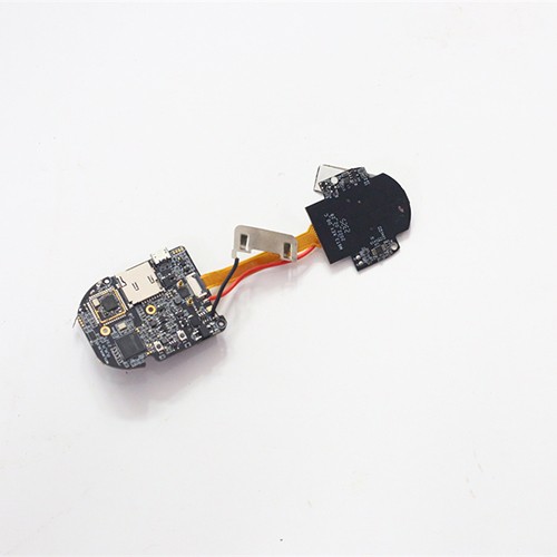
Frequency conversion equipment PCBA
- PCBA of frequency conversion equipment refers to assembling the electronic components (such as integrated circuits, resistors, capacitors, inductors, etc.) required for frequency conversion control on PCB through a specific process to form a circuit board assembly with frequency conversion control function.
VFD and Motor Drive PCBA
A variable frequency drive board is the clearest example of the two-sided problem in power electronics. One end of the board carries a microcontroller, gate drivers and feedback circuitry at fine pitch, where a few millivolts of noise matter. The other end carries the switching devices, the bus capacitors and the output terminals, where tens of amps are normal and heat is continuous. Both halves share one piece of laminate and one reflow profile.
What a drive assembly involves
- Fine-pitch placement for the control and gate-drive section, with components from 01005 upward at pitches down to 0.25 mm.
- Heavy copper power layers and thermal via arrays under the switching devices, agreed from the current and the allowable temperature rise.
- Wave or selective soldering for module pins, bus capacitors, shunts and output terminals, with selective soldering used where fine-pitch parts sit on the same board.
- Where required, a metal substrate, heatsink interface or thermal pad fitted and checked as part of the assembly.
- Conformal coating for boards installed in humid, dusty or condensing environments.
The thermal path is the electrical path
On a drive board, the copper that carries the motor current is usually the copper that carries the heat away from the switching device, and both requirements have to be satisfied by the same layout. That means the copper weight, the via array under the device and the interface to the heatsink or the enclosure are one decision rather than three. It also means the assembly process has to complete the joints on a board with a lot of metal in it: a profile that works on a lightweight control board will under-heat the joints under a large module, which is why the profile is developed for the specific board and verified where the design warrants it.
Noise, isolation and stability
Drive stability depends on details that live at the boundary between the two halves. The gate loop area, the way the current sense return is routed back to the controller, and the treatment of the isolation barrier between control and power all affect whether the drive runs cleanly or trips unpredictably under load. Those are design decisions, but assembly can protect or damage them: flux residue on a high-impedance feedback path, a poor joint on a shunt return, or a thermal profile that leaves a marginal joint under a power device will all show up as intermittent behaviour rather than as an obvious failure.
From schematic to a tested drive board
Send the Gerber files, the bill of materials, the quantity, the acceptance class and any environmental requirement such as coating or an operating temperature range. Where the programme involves a specific motor rating or a certification the product has to meet, stating it at quotation stage lets the assembly and inspection plan be written to match. The control-and-power split described here is shared with the inverter and energy storage range, where the same thermal, noise and isolation questions apply.
What actually limits a drive assembly
A variable frequency drive fails in the power stage far more often than in the control section, and most of the reasons are decided before assembly starts. Shoot-through occurs when the upper and lower switch in a half-bridge conduct at the same time; the dead-time inserted between them, and the timing of the gate drive that follows, set how much margin the design has. Assembly contributes to that margin through the gate loop. A gate trace that runs a long way from its driver, or a return path that shares copper with the switching current, adds inductance that appears as ringing on the gate and, in the worst case, as a spurious turn-on. Gate-drive layout is reviewed together with the customer's design, and the soldering route is chosen so the gate-drive side is not exposed to a second full thermal cycle.
Creepage, clearance and the copper that carries the current
On the power side the constraints are physical. Creepage and clearance across the isolation boundary follow the working voltage and the pollution degree the product is used in, and they are held by the layout rather than by the process. The copper then has to do two jobs at once: carry the motor current and take heat out of the switching devices. Depending on the design that means copper weights in the 2 to 10 oz range, thermal via arrays under the switching devices, and in some designs a metal-core or IMS structure. Press-fit pins, screw terminals and busbars bring the current in and out, and their joints — together with the pins of a power module — are the ones that need the heat, which is why selective soldering is used for the through-hole power content instead of a wave.
How a drive board is verified before it ships
Boards are built and inspected to IPC-A-610 Class 2 or Class 3 as agreed for the product. In-process inspection covers paste volume with SPI, placement and visible joints with AOI, and the joints under modules, QFNs and any hidden package with X-ray; electrical test covers in-circuit test and a functional test at board level. Where the specification calls for it, boards go through a loaded burn-in or an aging run at temperature, and thermal cycling between the working extremes — commonly -40 °C to +125 °C for industrial drives — is run as a qualification lot rather than on every board. End-of-line motor and dynamometer testing is normally carried out on the assembled unit at the customer's end; what is verified here is the board's own function, current draw and gate-drive behaviour at the interface.
Lead time and how to start
Prototype builds of a drive board typically take 5-8 working days and production quantities 2 to 5 weeks, depending on component availability and the mix of SMT and through-hole content. To quote, send the Gerber files, the BOM and the pick-and-place data through the contact page together with the working voltage and any thermal or safety requirement the product has to meet.
- Factory environment

What a drive board needs from the assembly process
Variable frequency drive boards: control and gate-drive sections at fine pitch, heavy copper power stages, current sensing and IGBT or module drive circuits, assembled with selective soldering for the through-hole power content and acceptance to Class 2 or Class 3.
Application
Each application area has its own assembly requirements. What changes from a medical instrument to a motor drive is the process, the acceptance class and the design rules that matter, and the pages below set out what is different about each one.