

PCB processing covers everything that happens to a bare board before it becomes a finished assembly: drilling, plating, etching, solder mask, surface finish and profiling, followed by electrical test. Process control at this stage decides the yield of everything that comes afterwards.
What the process covers
- Drilling and via formation, including controlled-depth and filled vias.
- Copper plating and etching against the specified trace and gap widths.
- Solder mask and silkscreen, and the surface finish the assembly process requires.
- Electrical test and final inspection before the boards move to assembly.
How it fits with assembly
Because fabrication and assembly sit in the same supply chain at Kilandu, surface finish, panelisation and fiducial placement can be planned around the SMT and DIP process from the start. Boards then run through 3D solder paste inspection, placement on the SMT lines, AOI on every board, X-ray where hidden joints are present, and functional test to your specification.
Process control at each step
Drilling, plating, etching and solder mask each have a window that determines whether the board that emerges is the board that was designed. Trace and gap widths are checked against the specified values rather than a tolerance of convenience, plating thickness in the barrels is controlled so that vias carry the current the design assumes, and solder mask registration is verified so that no pad is partially covered. Where controlled-impedance or high-speed nets are present, the stack-up and finish are agreed before the panel is released.
Why the processing and assembly stages are planned together
Several decisions only look correct in hindsight. Surface finish that suits hand soldering can degrade under multiple reflow passes. A panel that is efficient for fabrication may not suit the placement equipment. Fiducials and tooling holes that were added late may sit where the printer cannot reach them. Planning fabrication and assembly as one process removes those conflicts, which is only possible when both stages sit under the same roof.
Verification before assembly
Boards are electrically tested and visually inspected before release to the assembly lines, so a fabrication defect is caught while it is still a bare board rather than after components have been consumed. Once assembled, the board runs through 3D solder paste inspection, placement on the SMT lines, AOI, X-ray where hidden joints are present, and functional test to the customer's specification, with lot-level records retained throughout.
Previous:PCB manufacturing
-
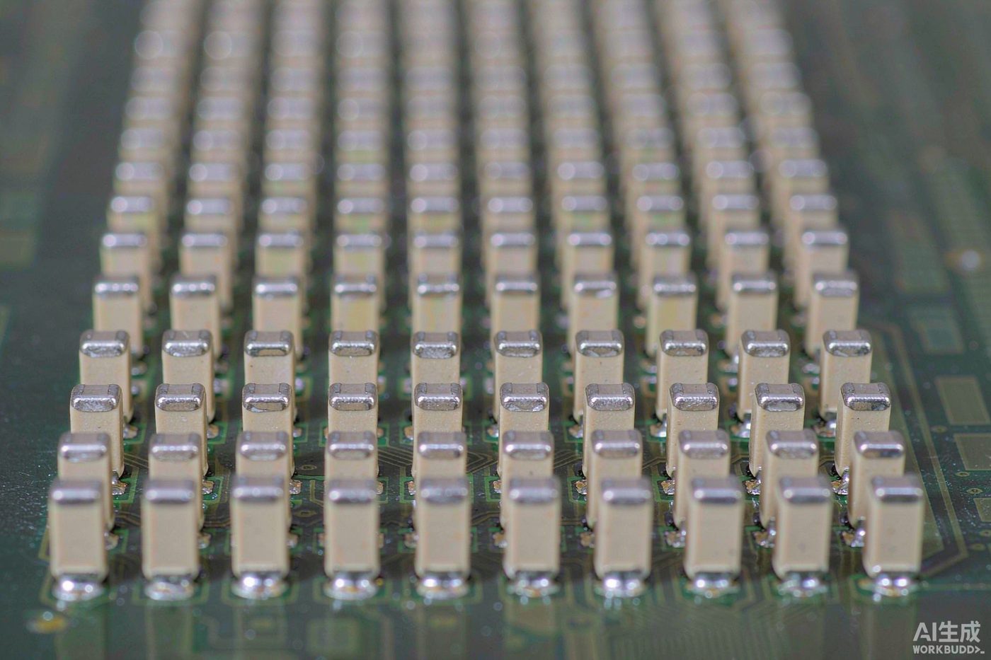
Passive Component Lead Times Are Rewriting PCBA Sourcing Decisions in 2026
-

A warm welcome to Mr. Jason Connor and Mr. David from Luxembourg for their guidance!
-

The PCBA Industry at the Start of 2026: AI Drives Market Surge, Intelligent Manufacturing and Material Upgrades Become the Main Themes
-

Connecting Infinite Possibilities | Bao'an District New Union 'Ignite Learning' Class (including our Shenzhen Jintianlei Innovation Technology Co., Ltd.) visited Biz Link to discuss new development op
-
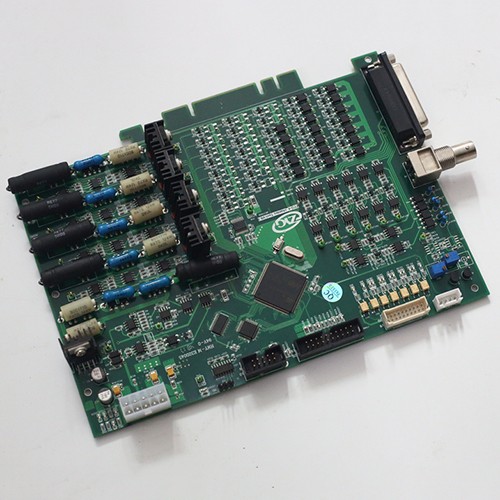
The core process of PCBA product customization
-
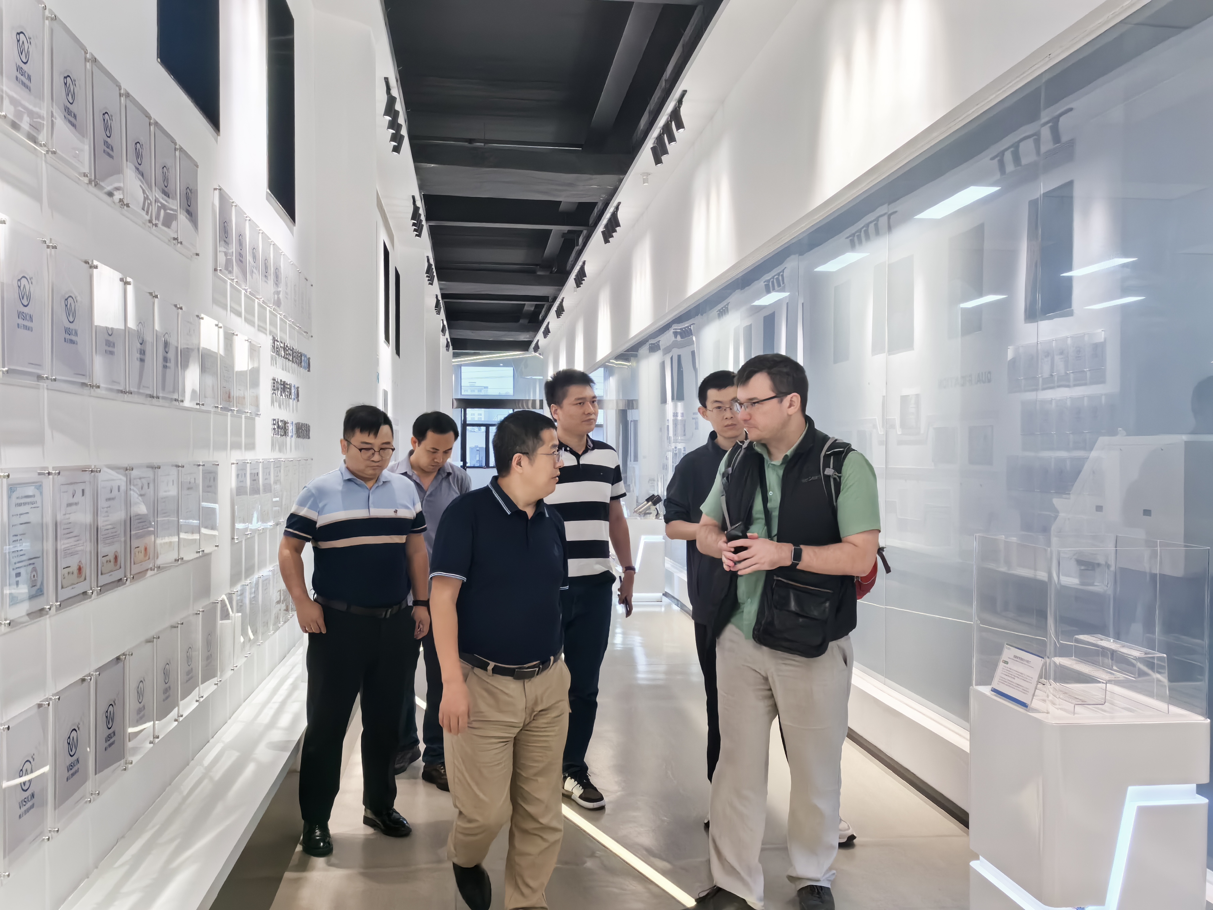
Welcome customers to visit our branch companies for factory inspection and guidance
-
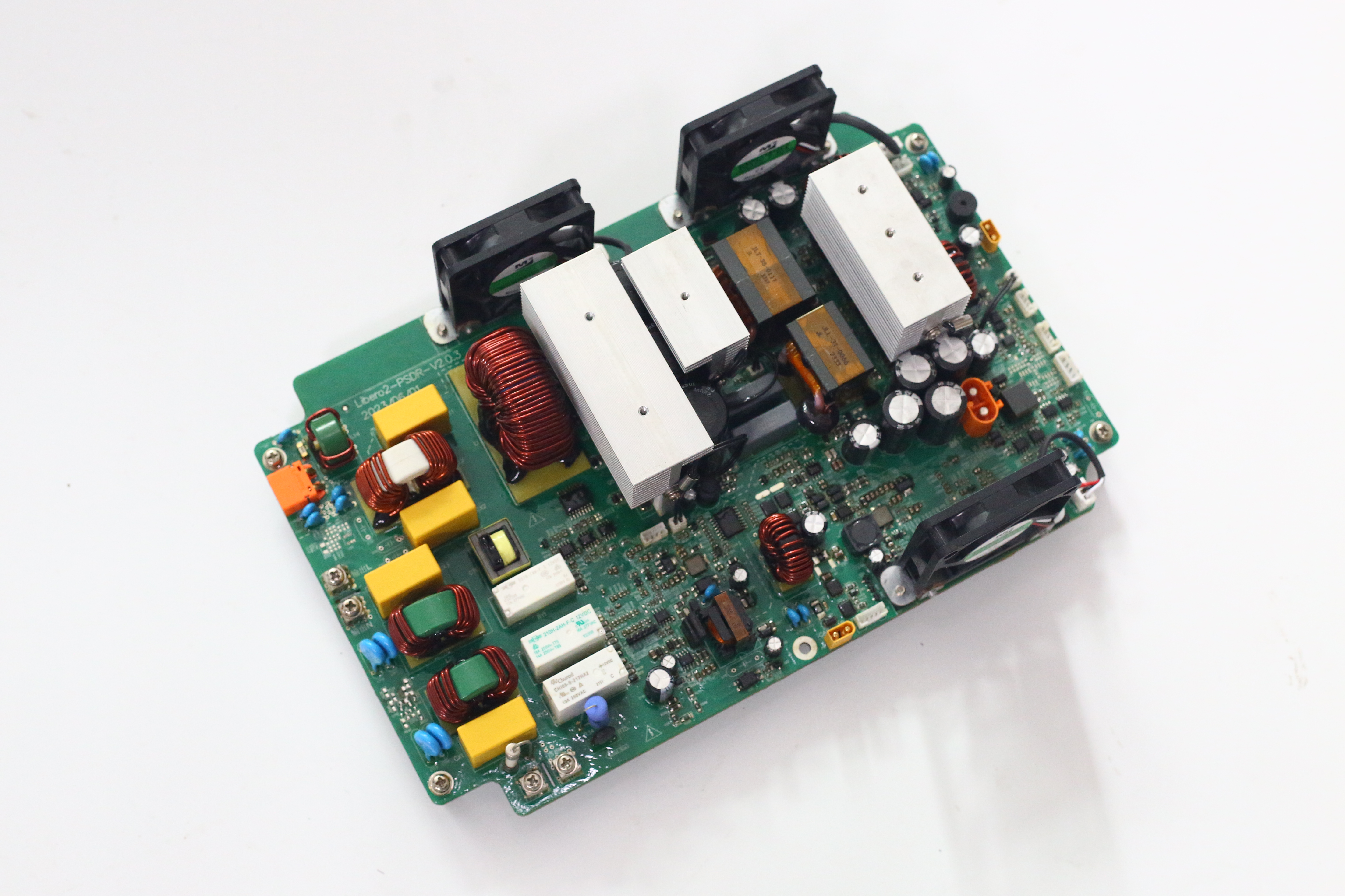
ExpeElectronica2024 in Munich, Germany
-
PCBA industry global prospects
-
Connecting Infinite Possibilities | Bao'an District New Union 'Ignite Learning' Class (including our Shenzhen Jintianlei Innovation Technology Co., Ltd.) visited Biz Link to discuss new development op
-
Explore the future trends of the PCBA industry! How can you make your production line more efficient with the help of intelligent technology?