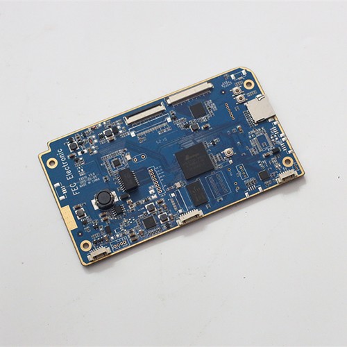

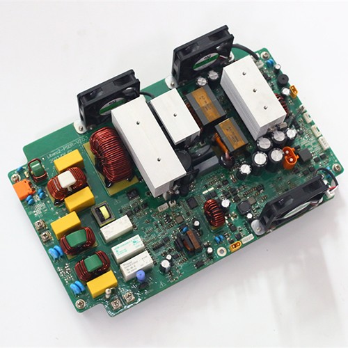
PCBA DIP processing
| PCBA DIP processing refers to the processing flow of Dual In-line Package, which is an important part of the PCBA assembly process, especially for those large or special components that cannot be installed by surface mount technology (SMT). |
PCBA DIP processing refers to the processing flow of Dual In-line Package, which is an important part of the PCBA assembly process, especially for large or special components that cannot be installed by surface mount technology (SMT).
The process flow of DIP processing usually includes the following steps:
1. Component pre-processing: Receive materials according to the BOM material list and perform pre-production pre-processing, such as foot cutting and molding. .
2. Plug-in: Manually insert the pre-processed components into the corresponding positions of the PCB board to prepare for the subsequent wave soldering.
3. Wave soldering: The plug-in PCB board passes through the wave soldering conveyor belt, and goes through the steps of spraying flux, preheating, wave soldering, cooling, etc. to complete the soldering.
4. Component foot cutting: Cut the feet of the soldered PCBA board to achieve the appropriate size.
5. Repair (post-welding): Repair and repair the PCBA finished boards that have been found to be incompletely welded.
6. Board cleaning: Remove the residual flux and other harmful substances on the PCBA finished products to achieve the cleanliness standard of environmental protection.
7. Functional test: Perform functional test on the welded PCBA finished boards to ensure that all functions are normal, and repair and retest the problems found.
Why Kilandu for turnkey PCBA and PCB
Turnkey, one factory
Gerber and BOM in, tested boards out: component sourcing, SMT, DIP, box-build and functional test under one roof in Shenzhen.
Production capacity
Line count, placement equipment and monthly capacity are documented on the factory capabilities page.
Quality system
Certificates, inspection stages and lot traceability are documented on the quality assurance page.
Markets and lead time
We supply OEM customers across Europe, Russia and the Americas; typical turnkey lead time is 2 to 5 weeks, depending on BOM complexity and component availability.
- Previous:PCBA DIP plug-in processing
Frequently asked questions
What exactly does Kilandu deliver for a custom PCBA project?
A turnkey service: we source the full bill of materials, fabricate the PCB, run SMT and DIP assembly, and finish with AOI, inspection and functional testing, so you receive tested, ready-to-install boards from one factory.
Which quality standards is the factory certified for?
Production follows IPC-A-610 Class 2/3 workmanship under a certified quality system, with RoHS and REACH compliant processes. The certificates and what each one covers are listed on the quality assurance page.
Which markets do you serve and how fast can you deliver?
We supply OEM customers across Europe, Russia and the Americas from our factory in Shenzhen, China, with typical turnkey lead times of 2 to 5 weeks depending on BOM complexity and volume.