
Customer requirement
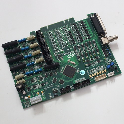
A PCB for medical imaging equipment on high-Tg, low-loss material: typically 6–10 layers, ~600 components, pilot build. Signal fidelity is paramount.
Manufacturing challenge
- Low-loss material and controlled impedance for imaging signals.
- ISO 13485 traceability and documentation are mandatory.
- FCT validates image-path integrity and noise floor.
Solution
Kilandu runs this board through a controlled NPI-to-production flow rather than a one-shot build:
- DFM: footprint, stack-up and test-point review is completed and fed back before any parts are ordered.
- Sourcing: turnkey procurement of the BOM, with qualified alternates managed for long-lead and obsolete parts.
- SMT: high-speed SMT lines with inline SPI, AOI and X-ray on BGA, voiding and hidden joints.
- Assembly: selective DIP for through-hole content and, where needed, conformal coating.
- Test: ICT for net integrity, then FCT for the board-specific functions above.
ISO 13485 process; AOI + X-ray; FCT on image path.
Result
First-article inspection to IPC-A-610 Class 2/3 is completed, a golden sample is retained as the release baseline, and a pilot run is signed off before mass production. Per-batch traceability (lot, AOI/X-ray records and ICT/FCT logs) is kept. Order quantities and the the customer specific acceptance result are confirmed per project.
Previous:High TG PCB
-
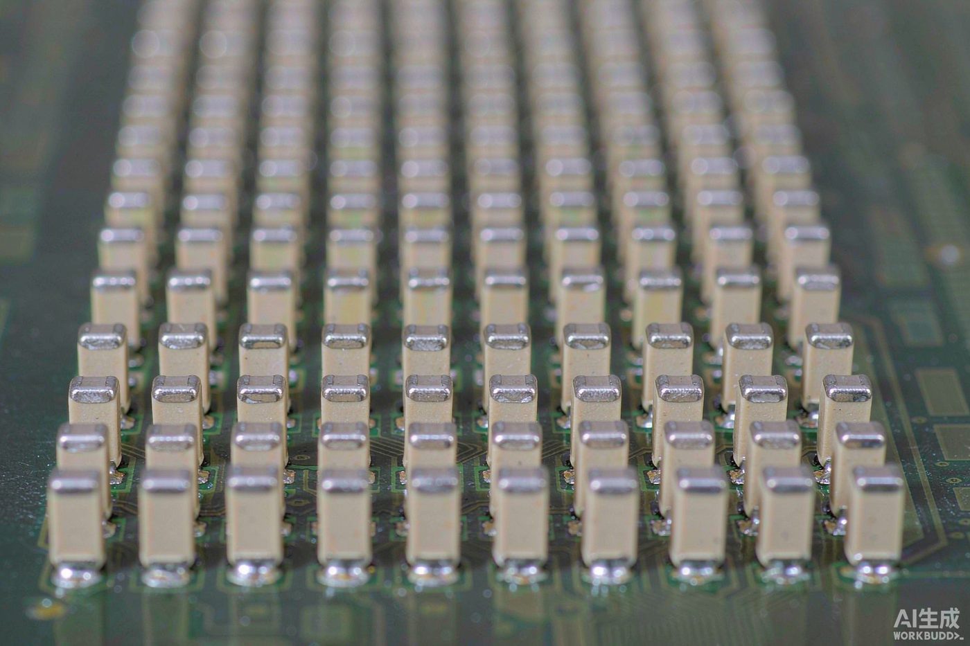
Passive Component Lead Times Are Rewriting PCBA Sourcing Decisions in 2026
-
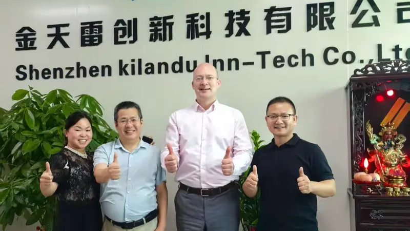
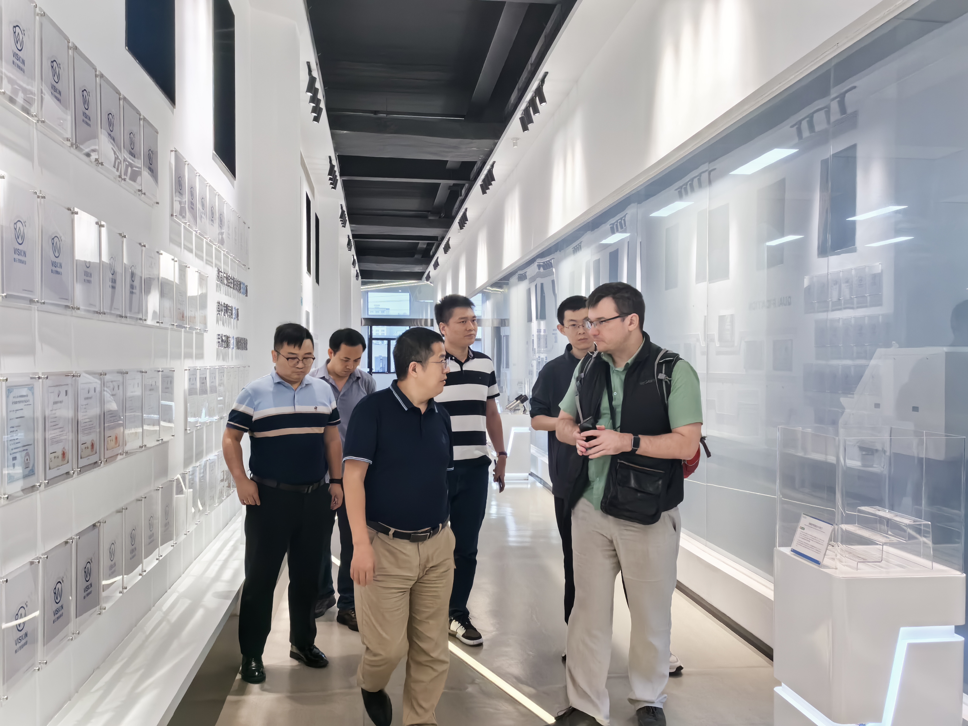
A warm welcome to Mr. Jason Connor and Mr. David from Luxembourg for their guidance!
-

The PCBA Industry at the Start of 2026: AI Drives Market Surge, Intelligent Manufacturing and Material Upgrades Become the Main Themes
-
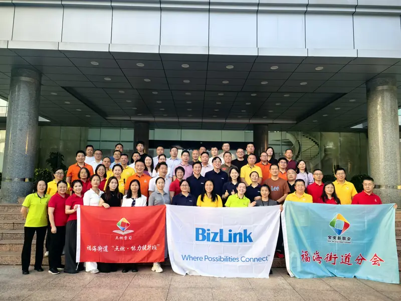
Connecting Infinite Possibilities | Bao'an District New Union 'Ignite Learning' Class (including our Shenzhen Jintianlei Innovation Technology Co., Ltd.) visited Biz Link to discuss new development op
-
The core process of PCBA product customization
-
Welcome customers to visit our branch companies for factory inspection and guidance
-
ExpeElectronica2024 in Munich, Germany
-
PCBA industry global prospects
-
Connecting Infinite Possibilities | Bao'an District New Union 'Ignite Learning' Class (including our Shenzhen Jintianlei Innovation Technology Co., Ltd.) visited Biz Link to discuss new development op
-
Explore the future trends of the PCBA industry! How can you make your production line more efficient with the help of intelligent technology?