

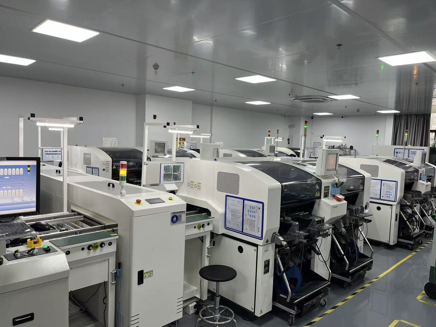
1. SMT patch (Surface Mount Technology)
Solder paste printing: Use a steel mesh to print solder paste evenly on the PCB pad.
Patch: Use a high-speed patch machine to accurately mount electronic components to the corresponding
pad position on the PCB.
Reflow soldering: Use a reflow oven to melt and cool the solder paste to form a reliable solder joint.
AOI inspection: Use automatic optical inspection equipment to check the soldering quality, such as whether
there are defects (false solder joints, bridging tin, missing parts, etc.).
2. DIP plug-in (Dual In-line Package) [For components that require plug-in]
Plug-in: Manual or automatic plug-in machines insert electronic components with pins (such as capacitors,
inductors, connectors, etc.) into through holes on the PCB.
Wave soldering: The PCB passes through a molten solder wave to fix the plug-in components.
Trimming and trimming: Trim off excess pins and trim solder joints.
3. Soldering and assembly
Manual soldering: For some special components (such as high-power devices and special interfaces),
manual soldering is required.
Cleaning: Remove residual flux and impurities during the welding process to improve the reliability of the
circuit board.
Assembly: Install additional components such as heat sinks, housings, shielding covers, etc.
4. Testing and quality inspection
Functional test (FCT): Check whether the functions of the PCBA are normal, such as voltage, current,
signal transmission, etc.
ICT test (In-Circuit Test): Check circuit parameters such as resistance, capacitance, inductance, IC pin connection,
etc. through test points.
Aging test: Test the stability and life of the PCBA under extreme environments such as high temperature and high
humidity.
5. Packaging and shipment
Protection treatment: Spray three-proof paint (moisture-proof, salt spray-proof, anti-static), etc. to ensure that the
PCBA is not affected by the environment during transportation and use.
Packaging: Use anti-static packaging materials to ensure that the PCBA is not damaged during transportation.
Delivery: Deliver the finished PCBA to the customer or use it for whole machine assembly.
Summary
PCB is just a bare board, while PCBA is a complete circuit board after a series of processes such as component
mounting, welding, and testing. PCBA can be directly used in various electronic devices, such as smart home,
automotive electronics, medical equipment, etc.
-
Passive Component Lead Times: What PCBA Buyers Should Check Before 2027
-

A warm welcome to Mr. Jason Connor and Mr. David from Luxembourg for their guidance!
-
The PCBA Industry at the Start of 2026: AI Drives Market Surge, Intelligent Manufacturing and Material Upgrades Become the Main Themes
-
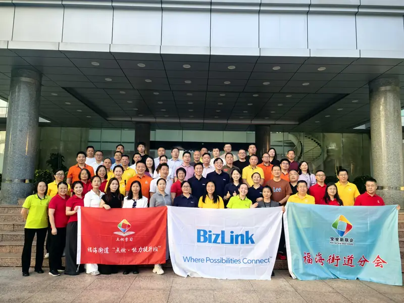
Connecting Infinite Possibilities | Bao'an District New Union 'Ignite Learning' Class (including our Shenzhen Jintianlei Innovation Technology Co., Ltd.) visited Biz Link to discuss new development op
-
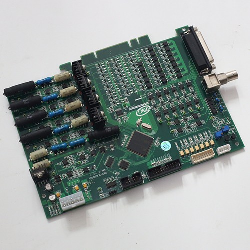
The core process of PCBA product customization
-
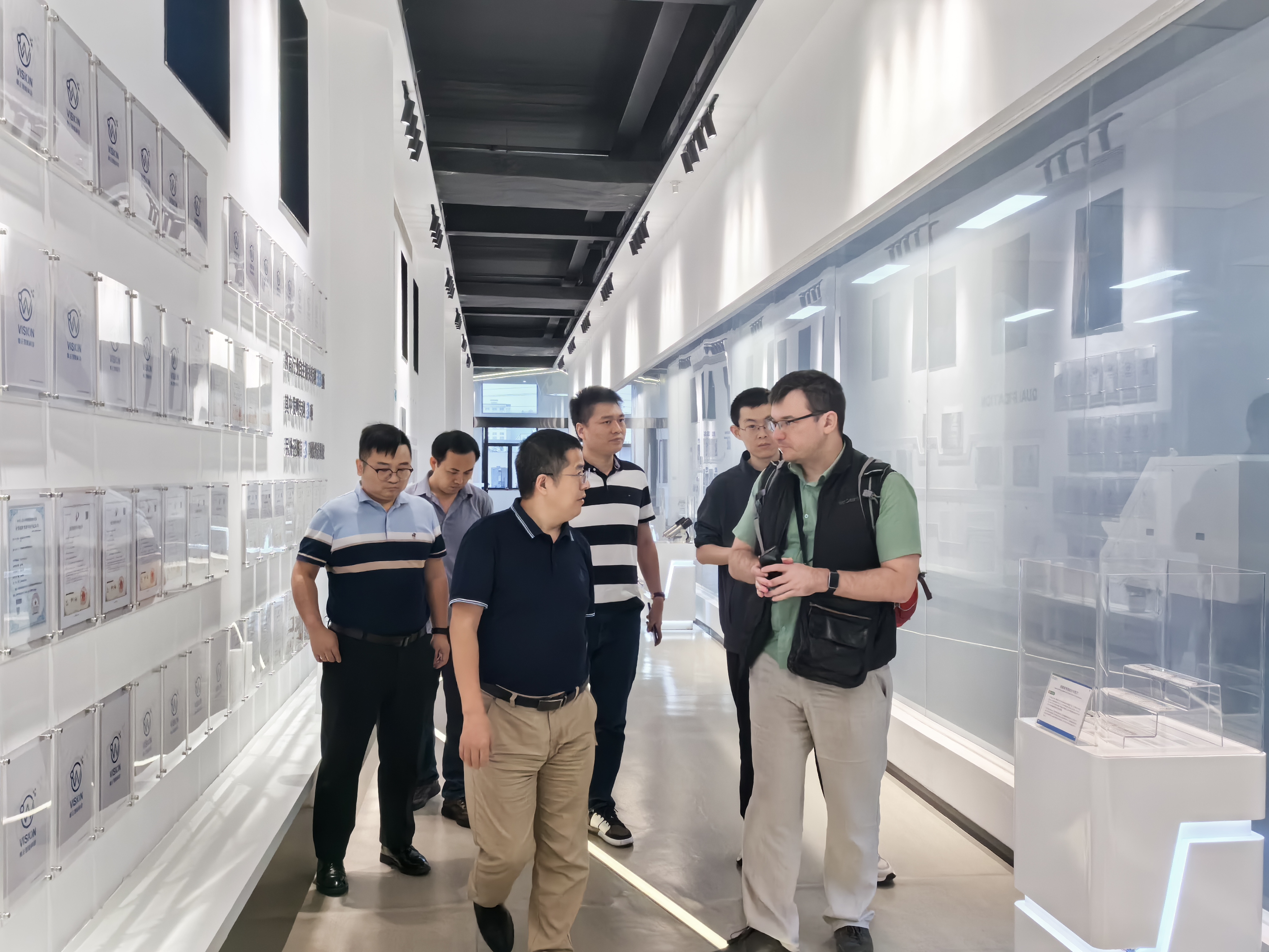
Welcome customers to visit our branch companies for factory inspection and guidance
-
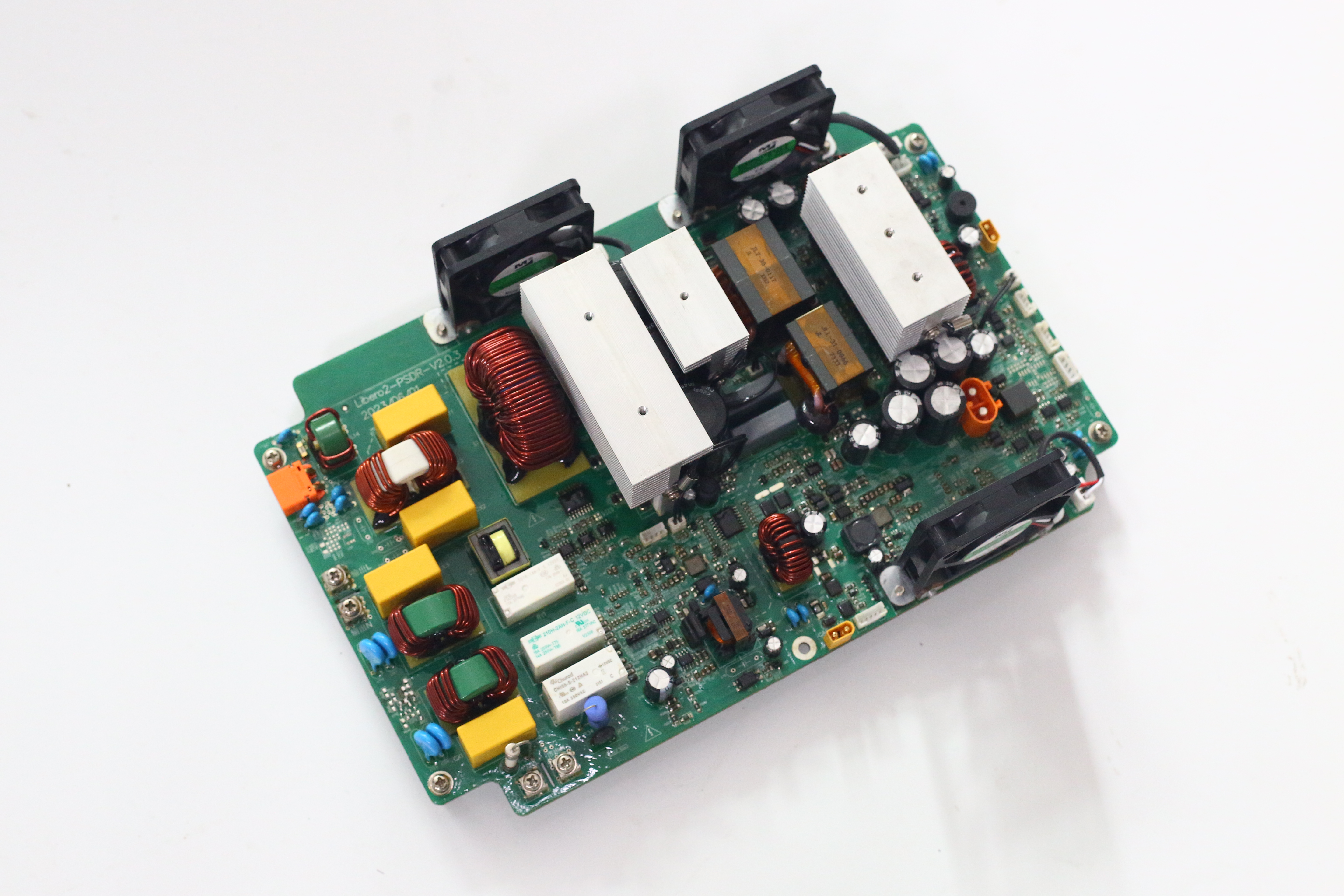
ExpeElectronica2024 in Munich, Germany
-
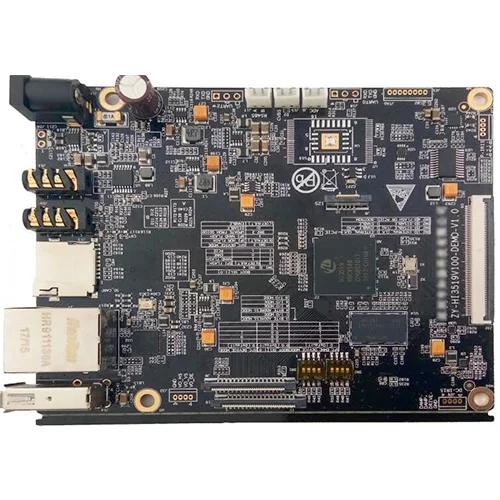
PCBA industry global prospects
-
Connecting Infinite Possibilities | Bao'an District New Union 'Ignite Learning' Class (including our Shenzhen Jintianlei Innovation Technology Co., Ltd.) visited Biz Link to discuss new development op
-
Explore the future trends of the PCBA industry! How can you make your production line more efficient with the help of intelligent technology?