
Multilayer PCB
| Product Category | Multilayer PCB |
|---|---|
| Material | KB6061, S1141, S1000, IT180, etc. |
| Number of layers | 4-48 layers/multilayer PCB |
| Solder Mask Color | Green |
| Silk Screen Color | White/Black |
| Finished Product Thickness | 0.3mm - 6.0mm |
| Copper Thickness | 0.5-6OZ |
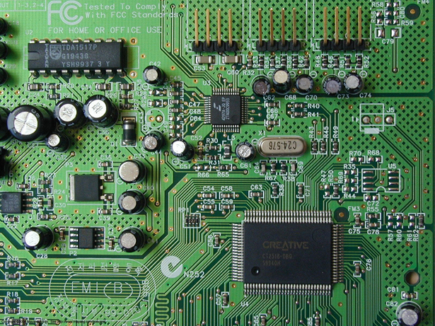
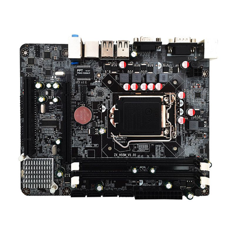
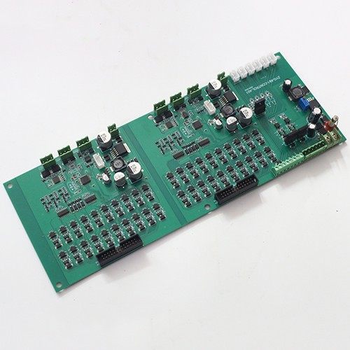
Multilayer PCB (Multilayer Printed Circuit Board) is a circuit board composed of three or more layers of conductive layers, which are interconnected through internal connection technology to achieve complex circuit design.
Features of Multilayer PCB:
1. High-density integration: Multilayer PCB can achieve more circuit connections in a limited space and improve the integration of circuits.
2. Excellent signal quality: Through reasonable inter-layer layout and signal line design, multi-layer PCB can effectively reduce interference and loss during signal transmission and improve signal quality.
3. Reduce electromagnetic interference (EMI): The design of multi-layer PCB can use the power layer and ground layer as shielding layers to reduce the impact of external electromagnetic fields on the circuit.
4. Improve thermal management performance: By distributing heat sources in different functional layers, multi-layer PCB can effectively dissipate heat and avoid local overheating.
Application fields of multi-layer PCB:
1. Communication equipment: such as smart phones, tablet computers, routers, etc., the high-density integration and excellent signal quality of multi-layer PCB make it the first choice for circuit design in these devices.
2. Automotive electronics: In automotive electronic control systems, multi-layer PCB can realize complex circuit control and signal processing.
3. Medical equipment: In medical electronic equipment, such as electrocardiographs, ultrasound machines, etc., the high-precision signal transmission and processing capabilities of multilayer PCBs have been widely used.
4. Industrial control: In industrial automation and control systems, multilayer PCBs can achieve efficient data acquisition and processing.
Why Kilandu for turnkey PCBA and PCB
Turnkey, one factory
Gerber and BOM in, tested boards out: component sourcing, SMT, DIP, box-build and functional test under one roof in Shenzhen.
Production capacity
Line count, placement equipment and monthly capacity are documented on the factory capabilities page.
Quality system
Certificates, inspection stages and lot traceability are documented on the quality assurance page.
Markets and lead time
We supply OEM customers across Europe, Russia and the Americas; typical turnkey lead time is 2 to 5 weeks, depending on BOM complexity and component availability.
Frequently asked questions
What exactly does Kilandu deliver for a custom PCBA project?
A turnkey service: we source the full bill of materials, fabricate the PCB, run SMT and DIP assembly, and finish with AOI, inspection and functional testing, so you receive tested, ready-to-install boards from one factory.
Which quality standards is the factory certified for?
Production follows IPC-A-610 Class 2/3 workmanship under a certified quality system, with RoHS and REACH compliant processes. The certificates and what each one covers are listed on the quality assurance page.
Which markets do you serve and how fast can you deliver?
We supply OEM customers across Europe, Russia and the Americas from our factory in Shenzhen, China, with typical turnkey lead times of 2 to 5 weeks depending on BOM complexity and volume.