

When a PCB is prepared for production, the question of how the individual boards are joined together has to be answered before the panel is released. A small board cannot be handled by the placement machine on its own, so several are processed as one panel and separated afterwards. The way they are separated is the connection method, and each option trades off handling strength against the finish of the board edge.
V-cut scoring
A V-shaped groove is cut into both sides of the panel along the separation line, leaving a thin web of material. The completed panel is then run through a depaneling machine or snapped by hand. Scoring is fast, adds almost no material cost and leaves a clean edge, but it requires a straight line across the full panel width and a board thickness that suits the process, usually around 0.6 to 1.6 mm. It cannot follow a curved outline and it consumes some panel area, since a strip either side is needed for the scoring tool.
Breakaway tabs and stamp holes
Instead of scoring, the board can be held by small tabs that are routed away at the intended break line, with a row of small drilled holes - often called mouse bites - forming the weak point. This works for irregular outlines and for boards that cannot be scored, and the tab positions can be placed where the board has no critical components. The trade-off is a rougher edge that may need cleaning, and small burrs that can interfere with a connector or a mounting face if the tab is badly placed.
Choosing between them
- Straight-sided boards in a normal thickness: V-cut is usually the simplest and cheapest.
- Curved or mixed outlines: routed tabs with break points.
- Boards carrying tall components close to the edge: check that the depaneling tool does not foul them.
- Any method: keep the separation line away from fine-pitch devices and from board edges that have to seat in a housing.
Why it matters to assembly
Panel design affects yield as much as it affects cost. A panel that warps under reflow heat carries every board on it out of position, and a separation line placed too close to a component can transmit stress into a solder joint when the panel is broken. Kilandu reviews panelisation before fabrication so that the separation method suits both the board outline and the assembly process, with assembly carried out on high-speed SMT and automatic DIP lines in Baoan District, Shenzhen; the equipment list is on the factory capabilities page.
-
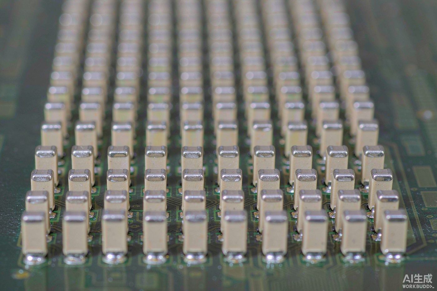
Passive Component Lead Times Are Rewriting PCBA Sourcing Decisions in 2026
-

A warm welcome to Mr. Jason Connor and Mr. David from Luxembourg for their guidance!
-

The PCBA Industry at the Start of 2026: AI Drives Market Surge, Intelligent Manufacturing and Material Upgrades Become the Main Themes
-
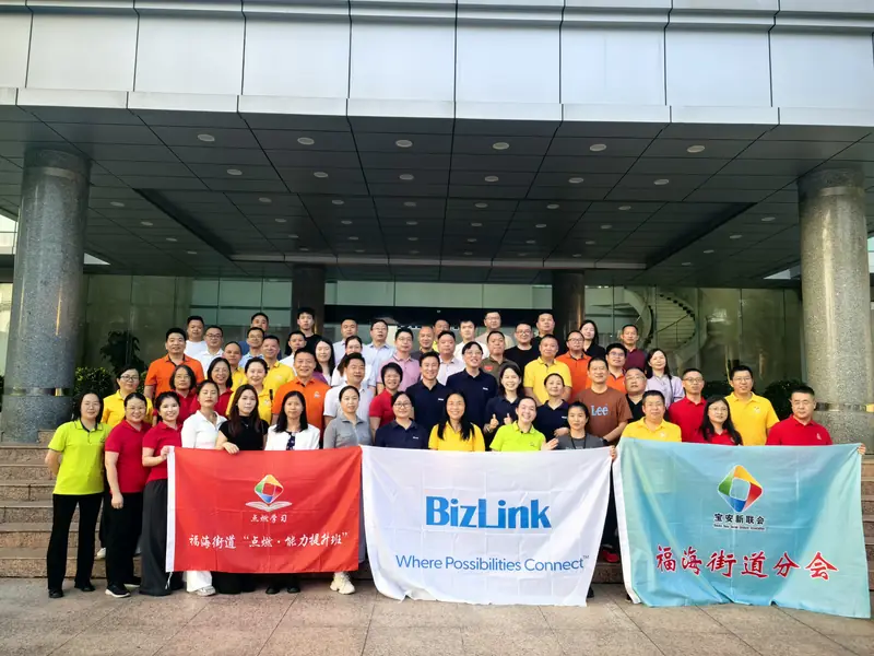
Connecting Infinite Possibilities | Bao'an District New Union 'Ignite Learning' Class (including our Shenzhen Jintianlei Innovation Technology Co., Ltd.) visited Biz Link to discuss new development op
-
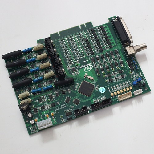
The core process of PCBA product customization
-
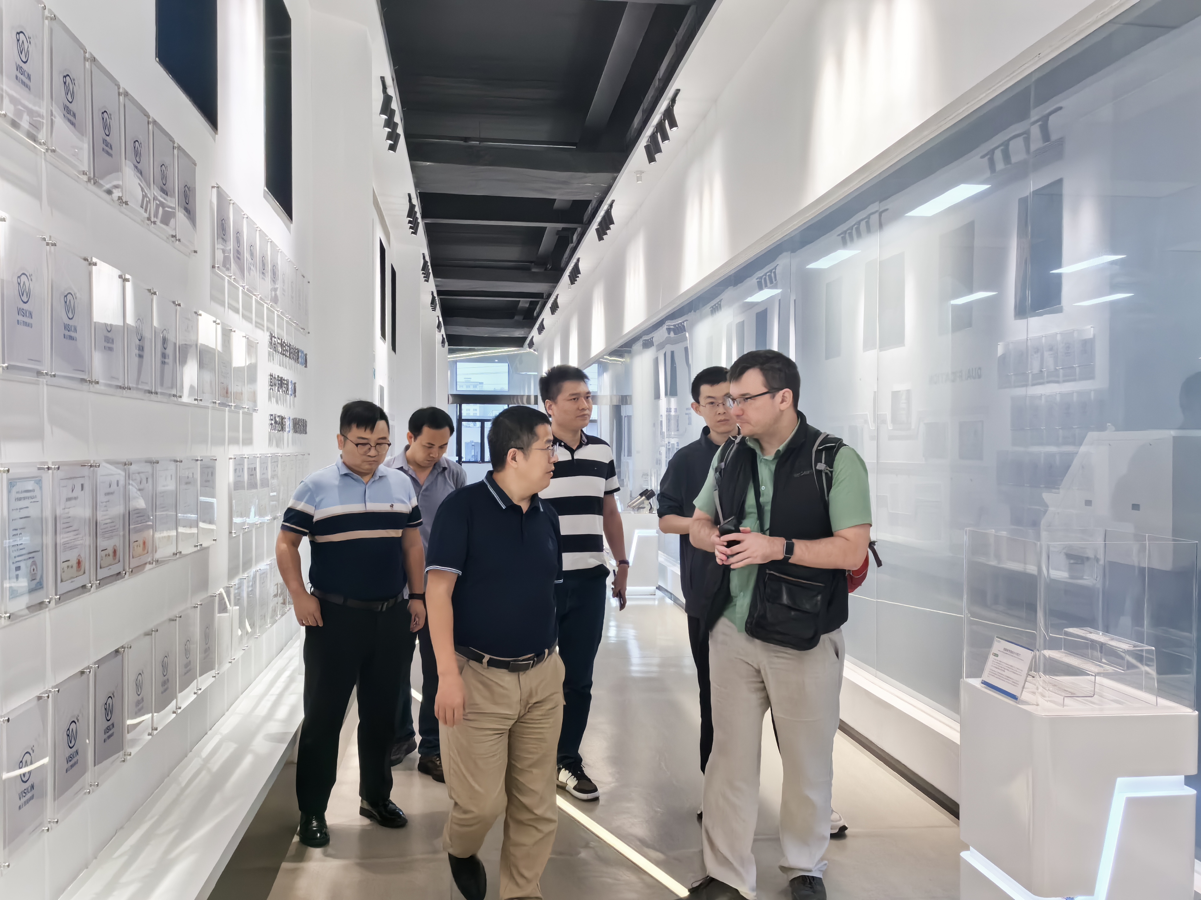
Welcome customers to visit our branch companies for factory inspection and guidance
-
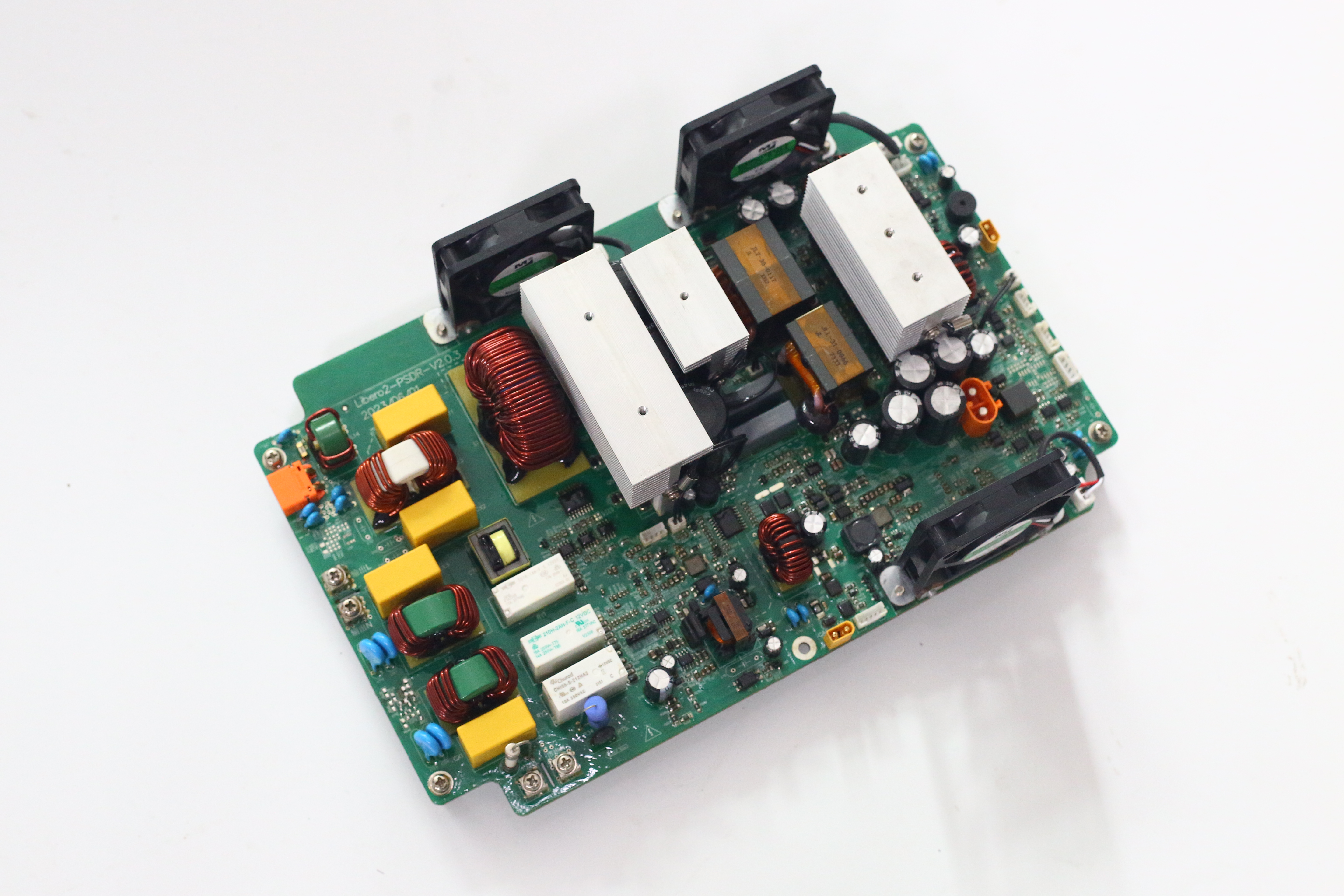
ExpeElectronica2024 in Munich, Germany
-
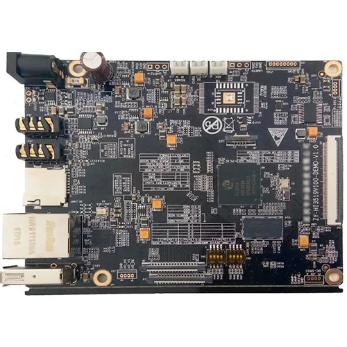
PCBA industry global prospects
-
Connecting Infinite Possibilities | Bao'an District New Union 'Ignite Learning' Class (including our Shenzhen Jintianlei Innovation Technology Co., Ltd.) visited Biz Link to discuss new development op
-
Explore the future trends of the PCBA industry! How can you make your production line more efficient with the help of intelligent technology?