
RF PCB
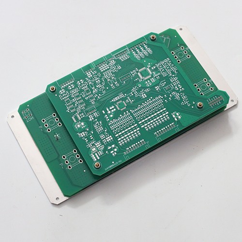
| Product Category | RF / High-Frequency PCB |
|---|---|
| Base material | FR-4 / Rogers 4350B / Rogers 4003C / Taconic / hybrid stackup |
| Layer count | 2-24 layers (sample: 4 layers) |
| Plate thickness | 1.6 +/- 0.25 mm |
| Board size | 225.00 mm x 112.00 mm (customizable) |
| Minimum aperture | 0.3 mm |
| Line width / spacing | 0.1 mm / 0.1 mm (4/4 mil) |
| Surface treatment | ENIG / HASL / Immersion Silver |
| Copper thickness | minimum hole copper 25 um, surface copper 1 oz |
| Frequency range | up to 20 GHz with controlled impedanc |
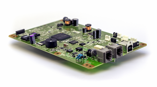
RF PCB is a printed circuit board used for the design and manufacture of radio frequency circuits, specializing in processing RF signals from hundreds of MHz up to tens of GHz. Kilandu fabricates RF and microwave boards on low-loss laminates (Rogers, Taconic, FR-4 hybrid) with controlled impedance, and provides turnkey SMT assembly for router, radar, and 5G applications.
RF PCB Capability
| Parameter | Capability |
|---|---|
| Layer count | 2-24 layers |
| Base material | FR-4 / Rogers 4350B / 4003C / Taconic / hybrid |
| Frequency range | Up to 20 GHz |
| Impedance control | +/- 10% (TDR tested every RF lot) |
| Surface finish | ENIG / Immersion Silver / HASL |
| Min line / space | 4 / 4 mil |
Applications
5G / telecom base-station and small-cell RF modules
Automotive radar and V2X antennas
RF routers, gateways, and wireless backhaul
IoT / LoRa / satellite communication boards
Frequently Asked Questions
What materials does Kilandu use for RF PCBs?
We run FR-4, Rogers (4350B/4003C), Taconic, and FR-4-Rogers hybrid stacks to balance loss, cost, and frequency needs.
Can you control impedance on RF boards?
Yes - controlled-impedance traces at +/-10% with TDR verification on every RF lot.
Do you offer RF PCB assembly (PCBA) too?
Yes, turnkey SMT + DIP + functional RF testing, with component sourcing from LCSC and global distributors.
Why Kilandu for turnkey PCBA and PCB
Turnkey, one factory
Gerber and BOM in, tested boards out: component sourcing, SMT, DIP, box-build and functional test under one roof in Shenzhen.
Production capacity
Line count, placement equipment and monthly capacity are documented on the factory capabilities page.
Quality system
Certificates, inspection stages and lot traceability are documented on the quality assurance page.
Markets and lead time
We supply OEM customers across Europe, Russia and the Americas; typical turnkey lead time is 2 to 5 weeks, depending on BOM complexity and component availability.
Frequently asked questions
What exactly does Kilandu deliver for a custom PCBA project?
A turnkey service: we source the full bill of materials, fabricate the PCB, run SMT and DIP assembly, and finish with AOI, inspection and functional testing, so you receive tested, ready-to-install boards from one factory.
Which quality standards is the factory certified for?
Production follows IPC-A-610 Class 2/3 workmanship under a certified quality system, with RoHS and REACH compliant processes. The certificates and what each one covers are listed on the quality assurance page.
Which markets do you serve and how fast can you deliver?
We supply OEM customers across Europe, Russia and the Americas from our factory in Shenzhen, China, with typical turnkey lead times of 2 to 5 weeks depending on BOM complexity and volume.