
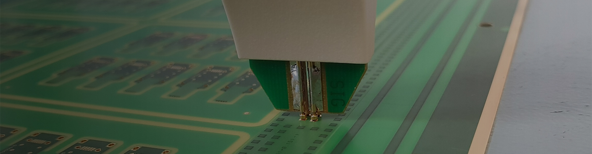
Short answer. An EV charger control board is a mixed-signal board with a mains-side power path and a low-voltage control side on the same substrate, so the specification that decides the build is isolation rather than placement density. Source it on four items: the creepage and clearance the design assumes, the current path and its thermal behaviour, the contactor or relay drive, and the test coverage that proves the protection actually operates.
Isolation is the specification, not a detail
The board carries the mains input, the metering front end, the controller and the communication interface. The distance between the mains side and the control side is fixed by the standard the charger is designed to, and it has to survive the assembly process unchanged. Two things follow for the assembler: no solder, flux or coating may bridge the isolation slot, and any conformal coating has to be applied with that slot masked rather than flowed over.
This is also where rework risk concentrates. A reworked joint near the isolation boundary can reduce the creepage distance without anyone noticing, which is why rework in that area should be defined at quotation rather than decided on the line.
The current path and its heat
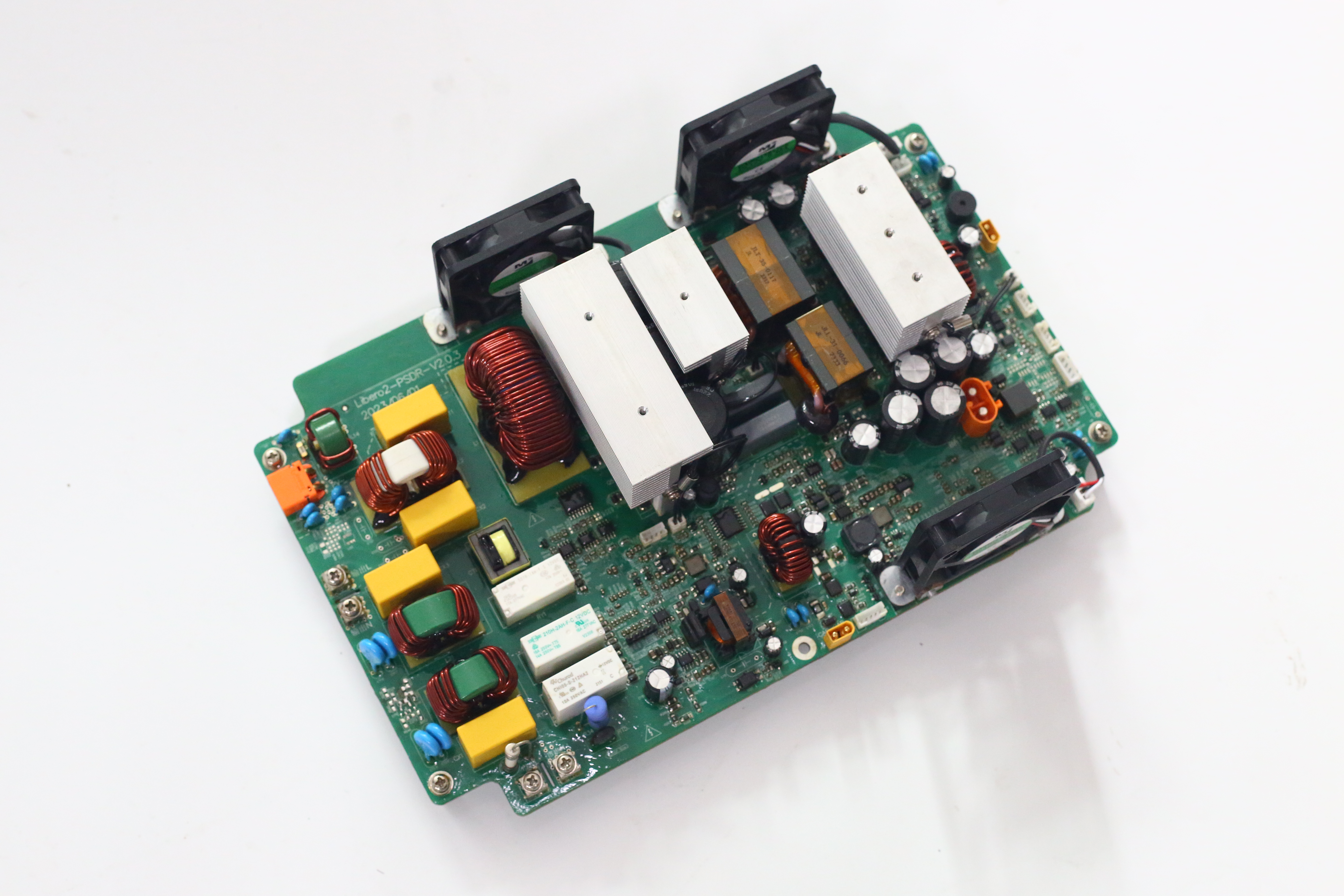
Relay and contactor terminals, shunt or current-transformer connections and the input connector all carry the full load current. On a 7 to 22 kW charger the joints at those terminals are thermal joints, and the assembly decision that matters is how they are soldered - selective solder, wave, or hand with a defined profile. A joint that looks acceptable optically can run hot under load, which is why a load test or a thermal check belongs in the first-article discussion.
What the control side needs from the build
- Contactor or relay drive. The driver stage switches an inductive load. Flyback and snubber components, and their placement relative to the driver, are part of what the build has to preserve.
- Metering front end. A shunt or current-transformer measurement path is a low-level analogue circuit sitting next to the switching node. Sense routing and analogue ground return decide whether the meter reads the current or the switching.
- Communication interface. Whether the charger speaks a serial protocol, a power-line scheme or a wireless module, the interface components and their isolation are part of the BOM that must not be substituted.
- Protection and residual-current sensing. These circuits are the ones a certification body will test, so they should be verified in functional test rather than assumed.
What to put in the test plan
Electrical test on a charger board typically covers in-circuit test on the assembled board and functional test of the control and protection functions. Where the design calls for dielectric withstand or insulation resistance verification, that requirement belongs in the test plan at quotation, with the voltage and duration stated, because it changes the fixture rather than the process. Programming and read-back should be recorded per unit on boards that carry firmware.
A supplier that offers only a power-on check has not tested a charger board. Protection behaviour is the function the product exists for.
Low to medium volume is a valid order size
Charger programmes often start at a few hundred units and stay there through a pilot phase. That volume is workable, but the cost structure is different from a volume run: setup, stencil, fixtures and programming are spread over fewer boards, and the practical minimum is set by the material packaging rather than by line time. The factors are set out on the MOQ and lead time page.
What Kilandu does on an EV charger build
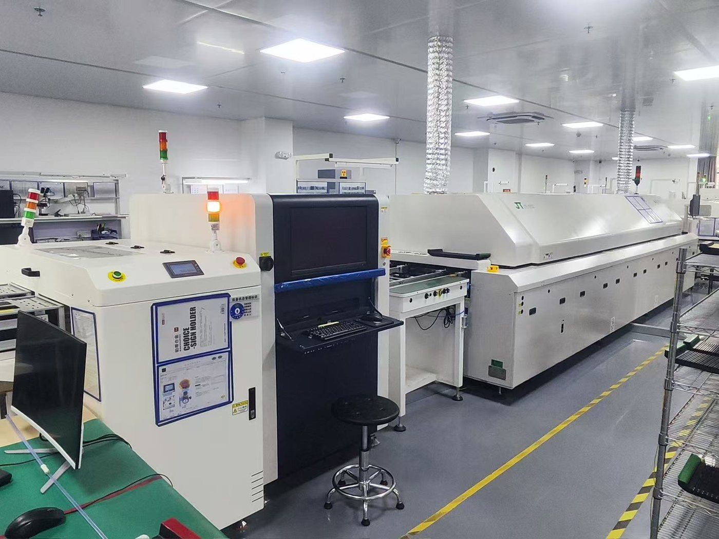
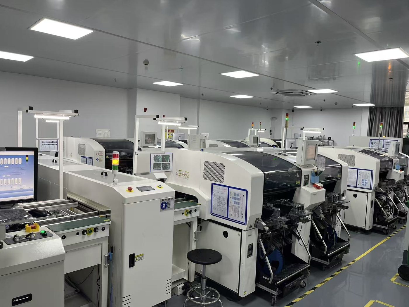
Kilandu assembles EV charger control boards in Shenzhen on four Yamaha SMT lines and three DIP lines, with SPI, AOI and X-ray in process and ICT plus FCT in electrical test. Mixed SMT and through-hole content, connector and terminal hardware, and conformal coating are handled in one flow, with coating applied after board-level test and before mechanical integration. Mass production is quoted at 2 to 5 weeks, prototypes at 5 to 8 working days, and repeat orders at 2 to 3 weeks.
Where the detail is documented
The application is described on the EV charger PCBA page and a build is written up on the EV charger case study page. Coating method and masking are covered on the conformal coating page. Send the schematic constraints, the isolation requirement and the target volume to alden@kilandu.com.


-

Welcome customers to visit our branch companies for factory inspection and guidance
-
ExpeElectronica2024 in Munich, Germany
-

Connecting Infinite Possibilities | Bao'an District New Union 'Ignite Learning' Class (including our Shenzhen Jintianlei Innovation Technology Co., Ltd.) visited Biz Link to discuss new
-
PCBA industry global prospects
-

Welcome French customer PACE to visit our factory for audit